LED package with light-absorbing layer

a technology of led packages and light-absorbing layers, which is applied in the direction of semiconductor/solid-state device manufacturing, electrical apparatus, semiconductor devices, etc., can solve the problems of reducing the size of led packages, reducing the light intensity, and increasing the cost of manufacturing led packages

Active Publication Date: 2013-10-29
ADVANCED OPTOELECTRONIC TECH INC
View PDF5 Cites 2 Cited by
  • Summary
  • Abstract
  • Description
  • Claims
  • Application Information

AI Technical Summary

Benefits of technology

[0010]Light emitted from the LED chip 18 is reflected by the reflector 14 in a certain predetermined direction so as to enhance the light intensity of the LED package 10. Even though the reflector 14 is physically thin, so that some light escapes through the reflector 14, the presence of the light-absorbing layer 15 around the reflector 14 reduces the effects of this escape of emitted light. Thus, the color rendering property of the LED package 10 is maintained, substantially without vignetting or halation during operation.

Problems solved by technology

However, in reducing the size of the LED packages the reflector has become thin, such that light emitted from the LED chip may be transmitted through the reflector, leading to a reduction in the light intensity and reduced ability to render color(s).
To avoid these limitations, increasing the thickness of the reflector or coating the reflector with a metallic layer are possible; nevertheless, these methods present obstacles to the reduction in size of an LED package, and the cost of manufacturing the LED packages is thereby increased.

Method used


Image

  • LED package with light-absorbing layer
  • LED package with light-absorbing layer
  • LED package with light-absorbing layer

Examples


Embodiment Construction

[0006]Exemplary embodiments of the disclosure will now be described with reference to the accompanying drawings.

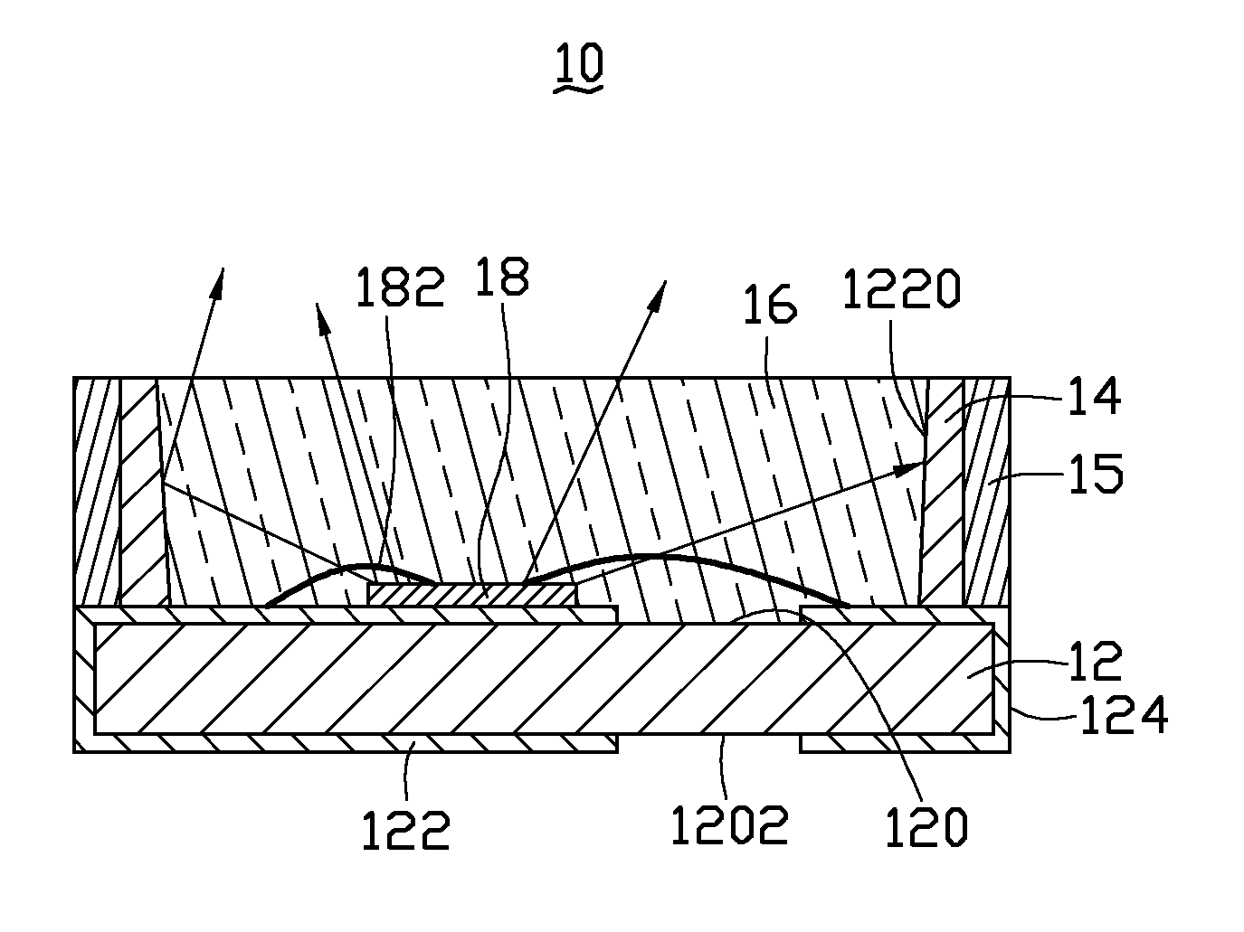
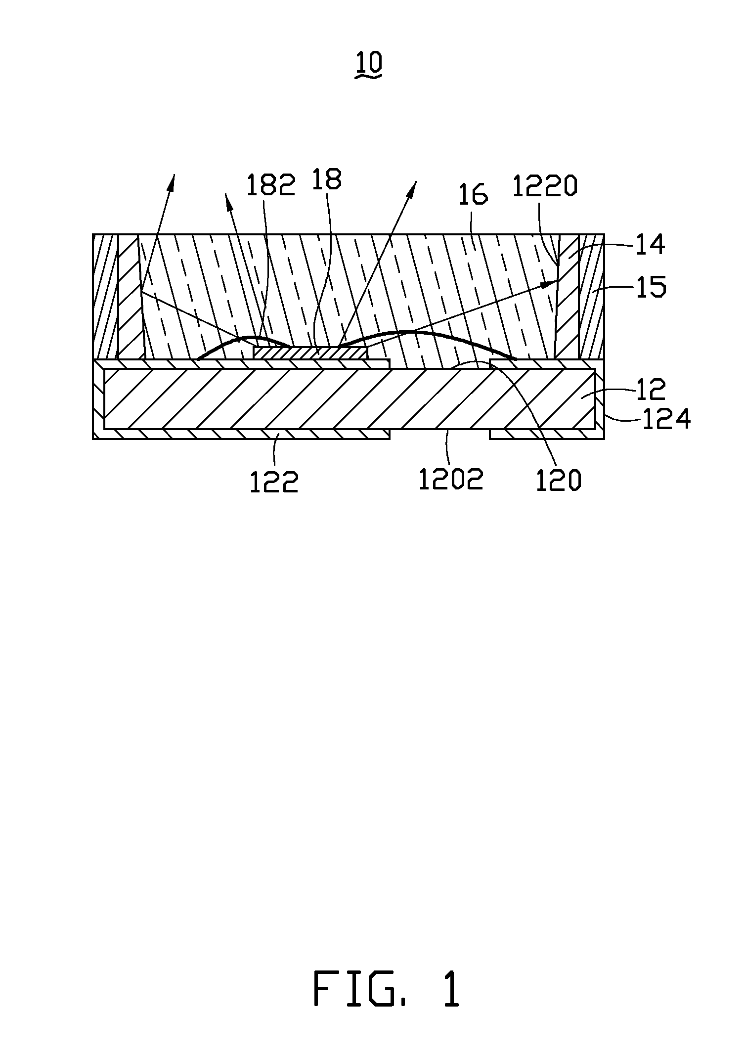
[0007]Referring to FIG. 1, the disclosure provides a first embodiment of an LED package 10, comprising a substrate 12, a reflector 14, a light-absorbing layer 15, an encapsulation layer 16 and an LED chip 18.

[0008]The substrate 12 comprises two electrodes 122, 124 located thereon, wherein the two electrodes 122, 124 comprise a cathode and an anode respectively, and the substrate 12 has a top surface 120 and a bottom surface 1202. Each of the two electrodes 122, 124 extends from the top surface 120 to the bottom surface 1202 of the substrate 12. In this embodiment, the LED chip 18 is disposed on the electrode 122 and makes electrical connection with the two electrodes 122, 124 via conductive wires 182. Thus, the LED chip 18 is able of emitting light by current from the two electrodes 122, 124.

[0009]The reflector 14 is located on the substrate 12, defining a depression 1220 ...


PUM


Abstract

An LED package comprises a substrate, a reflector, a light-absorbing layer, an encapsulation layer and an LED chip. The light-absorbing layer is located around the reflector and is able to absorb any light which penetrates through the reflector. Therefore, any vignetting or halation of light from the LED package is prevented. Moreover, the LED package can be constructed on a very small scale with no reduction in its color rendering properties.

Description

TECHNICAL FIELD[0001]The disclosure relates generally to light emitting diode (LED) package, and more particularly to an LED package having light-absorbing structure.DESCRIPTION OF THE RELATED ART[0002]LEDs are popular due to low power consumption, high efficiency, quick reaction time, long life and the absence of toxic elements such as mercury. Generally, a reflector is allocated inside an LED package to increase the light intensity and render the desired color(s), wherein the reflector is made of polyphthalamide (PPA) or other thermoplastic materials. However, in reducing the size of the LED packages the reflector has become thin, such that light emitted from the LED chip may be transmitted through the reflector, leading to a reduction in the light intensity and reduced ability to render color(s). To avoid these limitations, increasing the thickness of the reflector or coating the reflector with a metallic layer are possible; nevertheless, these methods present obstacles to the re...

Claims


Application Information

Patent Timeline
Patent Type & Authority Patents(United States)
IPC IPC(8): H01L33/00H01L21/00
CPCH01L33/486H01L33/60H01L2933/0033H01L2224/48091H01L2224/48227H01L2924/00014
Inventor HU, PI-CHIANGHSU, SHIH-YUANWANG, KAI-LUN
Owner ADVANCED OPTOELECTRONIC TECH INC
Why Eureka
Try Eureka