Level shifter circuit and gate driver circuit including the same

a level shifter circuit and gate driver technology, applied in logic circuit coupling/interface arrangement, pulse technique, instruments, etc., can solve the problems of low operating speed of pulse transformers and malfunctions, and achieve the effect of preventing malfunction of gain conversion units and stable operation

Inactive Publication Date: 2014-01-07
SAMSUNG ELECTRO MECHANICS CO LTD
View PDF14 Cites 0 Cited by
  • Summary
  • Abstract
  • Description
  • Claims
  • Application Information

AI Technical Summary

Benefits of technology

[0010]An aspect of the present invention provides a level shifter circuit including a gain conversion unit including a current mirror circuit able to operate stably even when reference voltage of high side gate driver circuit drops to have a negative (−) potential, and a noise removal unit capable of preventing malfunctioning of the gain conversion unit when a sudden fluctuation in voltage occurs.
[0011]According to an aspect of the present invention, there is provided a level shifter circuit including: a plurality of switching devices connected to a predetermined DC power supply through a resistor and operated by different driving signals; a gain conversion unit operated by first signals output from the plurality of switching devices, respectively, and generating second signals having a level within a predetermined range of the first signals; and a noise removal unit connected to at least one output terminal among the plurality of switching devices to prevent malfunctioning of the gain conversion unit, wherein the gain conversion unit inputs the second signals to a high side gate driver circuit through an inverter circuit.
[0018]According to another aspect of the present invention, there is provided a level shifter circuit including: a first transistor and a second transistor controlled so as to be turned-on and turned-off by a first pulse signal and a second pulse signal having different phases; a first resistor and a second resistor respectively connected between drain terminals of the first transistor and the second transistor and a predetermined DC power supply; a third transistor connected to the drain terminal of the first transistor; a fourth transistor connected to the drain terminal of the second transistor; and a first current mirror circuit having an input terminal connected to a drain terminal of the third transistor and an output terminal connected to a drain terminal of the fourth transistor, wherein the fourth transistor prevents output fluctuations in the first current mirror circuit due to a voltage drop occurring in at least one of the first resistor and the second resistor by a change in the DC power supply.
[0019]The level shifter circuit may further include: a fifth transistor connected to the drain terminal of the second transistor; a sixth transistor connected to the drain terminal of the first transistor; and a second current mirror circuit having an input terminal connected to a drain terminal of the fifth transistor and an output terminal connected to a drain terminal of the sixth transistor, wherein the sixth transistor prevents output fluctuations in the second current mirror circuit due to a voltage drop occurring in at least one of the first resistor and the second resistor due to the change in the DC power supply.

Problems solved by technology

However, the pulse transformer has a low operating speed and thus, a level shifter circuit has mainly been used for a high side gate driver circuit.
In this case, malfunctions may occur in the high side gate driver circuit when the level of the output signal is only changed to a ground level, in the case in which a level of the output signal applied to the input terminal of the inverter drops to have a negative (−) potential from a potential of a reference voltage of the high side gate driver circuit.

Method used


Image

  • Level shifter circuit and gate driver circuit including the same
  • Level shifter circuit and gate driver circuit including the same
  • Level shifter circuit and gate driver circuit including the same

Examples


Embodiment Construction

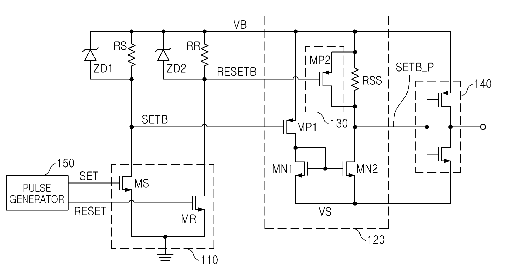
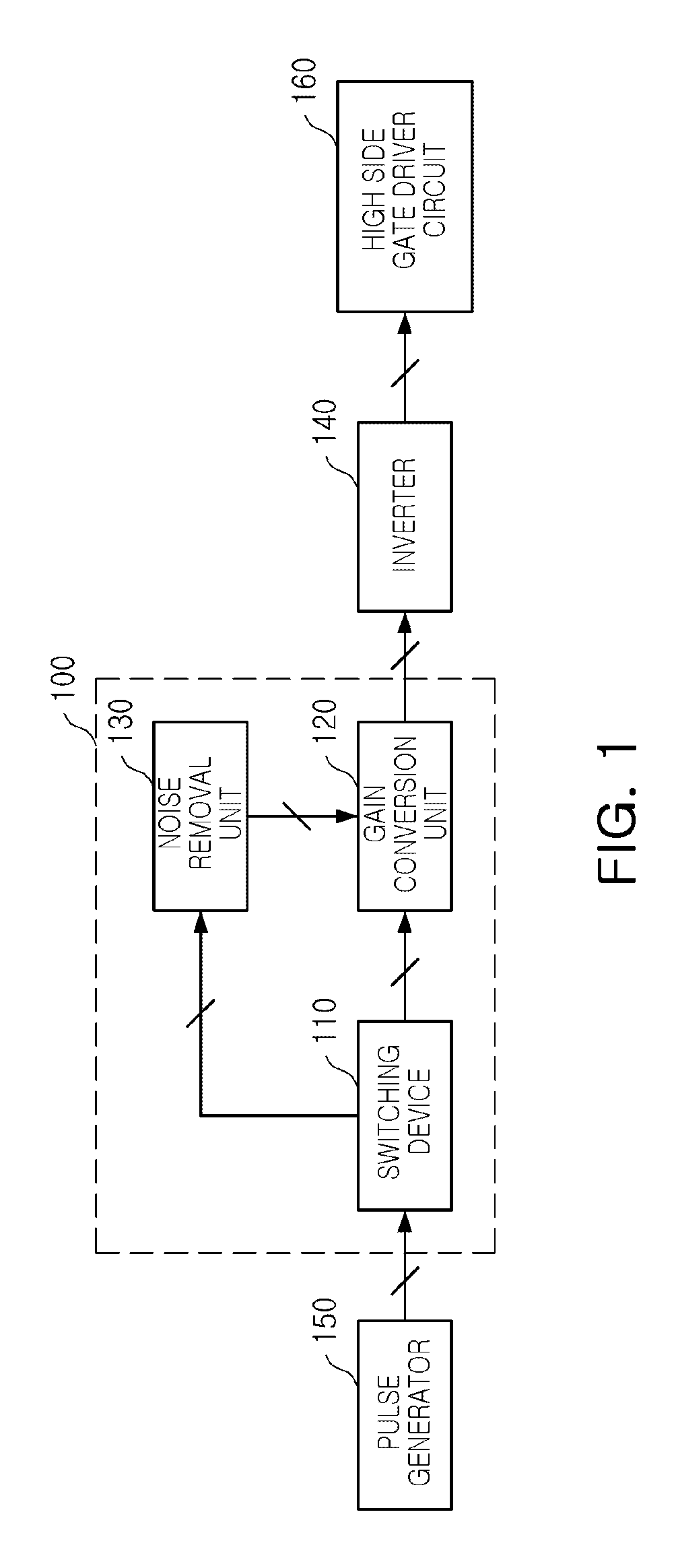
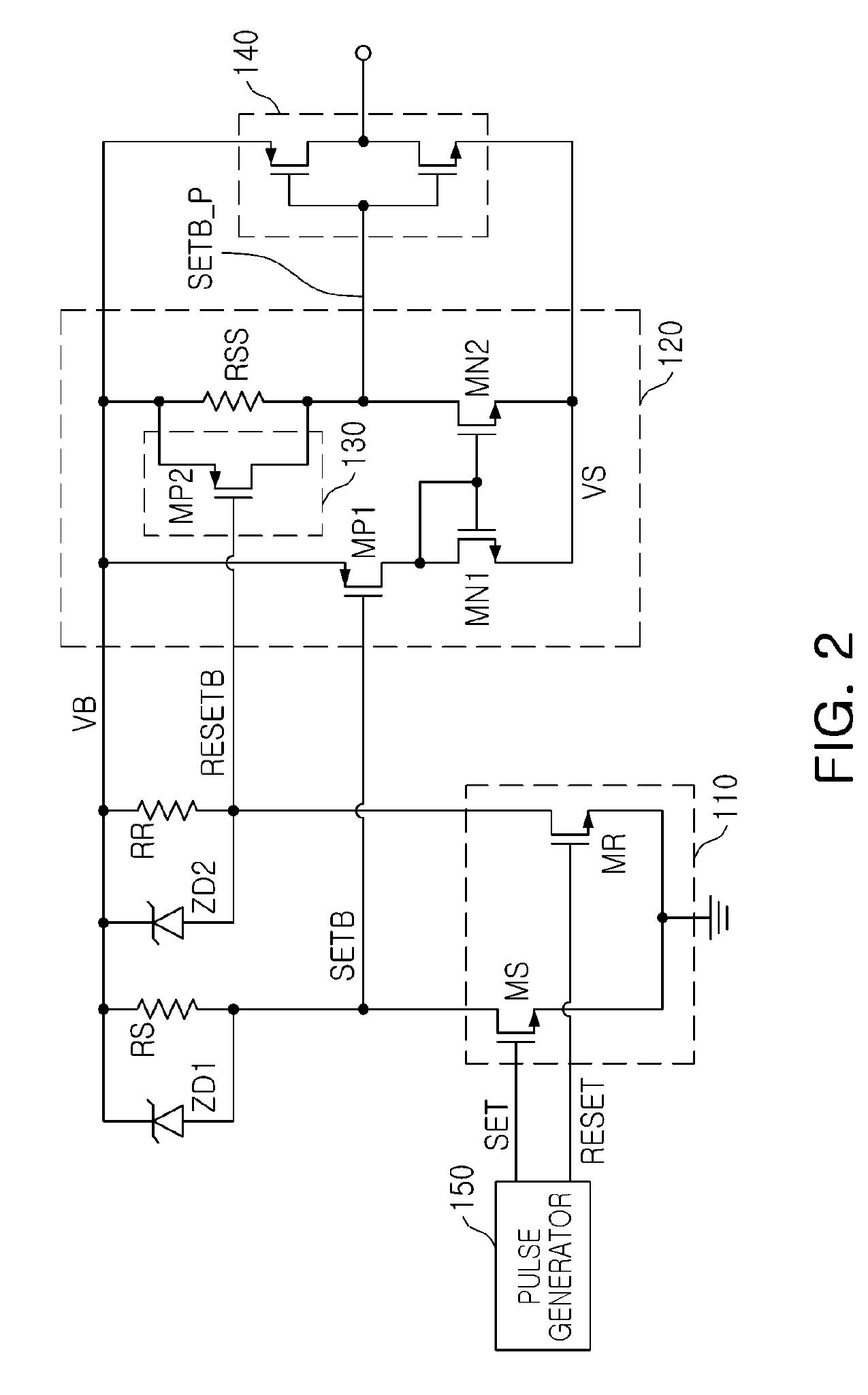
[0031]Embodiments of the present invention will be described in detail with reference to the accompanying drawings. These embodiments will be described in detail to allow those skilled in the art to practice the present invention. It should be appreciated that various embodiments of the present invention are different but are not necessarily exclusive. For example, specific shapes, configurations, and characteristics described in an embodiment of the present invention may be implemented in another embodiment without departing from the spirit and the scope of the present invention. In addition, it should be understood that positions and arrangements of individual components in each disclosed embodiment may be changed without departing from the spirit and the scope of the present invention. Therefore, the detailed description described below should not be construed as being restrictive. In addition, the scope of the present invention is defined only by the accompanying claims and thei...


PUM


Abstract

There are provided a level shifter circuit and a gate driver circuit including the same. The level shifter circuit includes: a plurality of switching devices connected to a predetermined DC power supply through a resistor and operated by different driving signals; a gain conversion unit operated by first signals output from the plurality of switching devices, respectively, and generating second signals having a level within a predetermined range of the first signals; and a noise removal unit connected to at least one output terminal among the plurality of switching devices to prevent malfunctioning of the gain conversion unit, wherein the gain conversion unit inputs the second signals to a high side gate driver circuit through an inverter circuit.

Description

CROSS-REFERENCE TO RELATED APPLICATIONS[0001]This application claims the priority of Korean Patent Application No. 10-2012-0058072 filed on May 31, 2012, in the Korean Intellectual Property Office, the disclosure of which is incorporated herein by reference.BACKGROUND OF THE INVENTION[0002]1. Field of the Invention[0003]The present invention relates to a level shifter circuit capable of preventing malfunctions from occurring due to sudden voltage fluctuations while being stably operated even when a range of an operating voltage has a negative potential, and a gate driver circuit including the same.[0004]2. Description of the Related Art[0005]A level shifter circuit is a circuit shifting an on / off signal that is a control signal having a low voltage level to have a high or low voltage level in a high side gate driver circuit. In order to drive a switching device such as a high side insulated gate bipolar transistor (IGBT) or a metal-oxide-semiconductor field-effect transistor (MOSFET...

Claims


Application Information

Patent Timeline
Patent Type & Authority Patents(United States)
IPC IPC(8): H03L5/00
CPCH03K19/00361H03K19/0185H03K19/018528G09G3/20H03K19/0175
Inventor PANG, SUNG, MAN
Owner SAMSUNG ELECTRO MECHANICS CO LTD
Why Eureka
Try Eureka