

Multi-cell per memory-bit circuit and method
a memory-bit and multi-cell technology, applied in the field of memory-integrated circuits, can solve the problems of insufficient current to carry out a write “0” operation, data loss, and inability to provide enough current to carry out a write “1” operation,
- Summary
- Abstract
- Description
- Claims
- Application Information
AI Technical Summary
Benefits of technology
Problems solved by technology
Method used
Image

Examples
Embodiment Construction
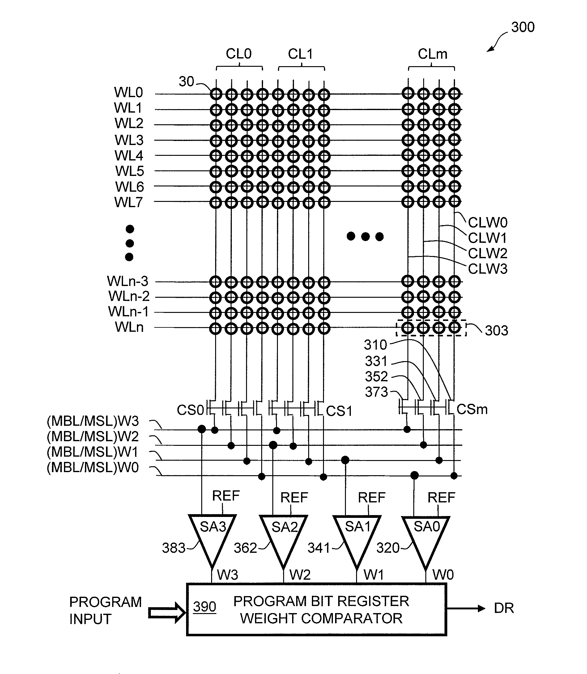
[0055]During write operation, a memory cell may exhibit randomly different write times at different occasions even under the same, stable conditions. Such behavior may not result from wear-out mechanisms that could be screened out during factory testing, but instead, results from probabilistic behavior of the memory cell's write characteristics. Memory cells determined to be defective for non-probabilistic reasons may be removed from a cell population by testing at the factory (by the seller) to scrap bad chips or repair defects by replacing defective cells with redundant cells on-chip during the memory repair step. However, the remaining population may still exhibit probabilistic behavior. Alternatively, after factory shipment to the field and if the chip is in regular use by the end-user, memory systems may be able to flag address locations corresponding to slow to write cells, mapping them out of the usable address space. The end-user mapping of slow to write cells results in a d...
PUM
 Abstract
Description
Claims
Application Information