
Methods, systems, and apparatus for timing and signal integrity analysis of integrated circuits with semiconductor process variations

a technology of integrated circuits and process variations, applied in computer aided design, program control, instruments, etc., can solve problems such as changes in performance and yield, design and manufacturing of semiconductor integrated circuits,

Active Publication Date: 2014-01-14
CADENCE DESIGN SYST INC
View PDF6 Cites 8 Cited by
  • Summary
  • Abstract
  • Description
  • Claims
  • Application Information

AI Technical Summary

Problems solved by technology

Designing and manufacturing semiconductor integrated circuits is a challenge.
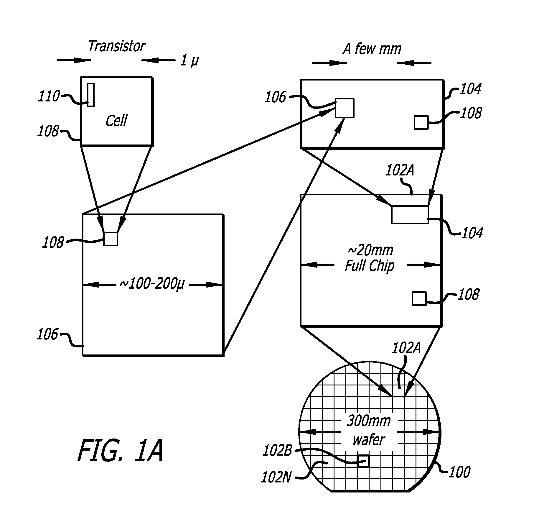
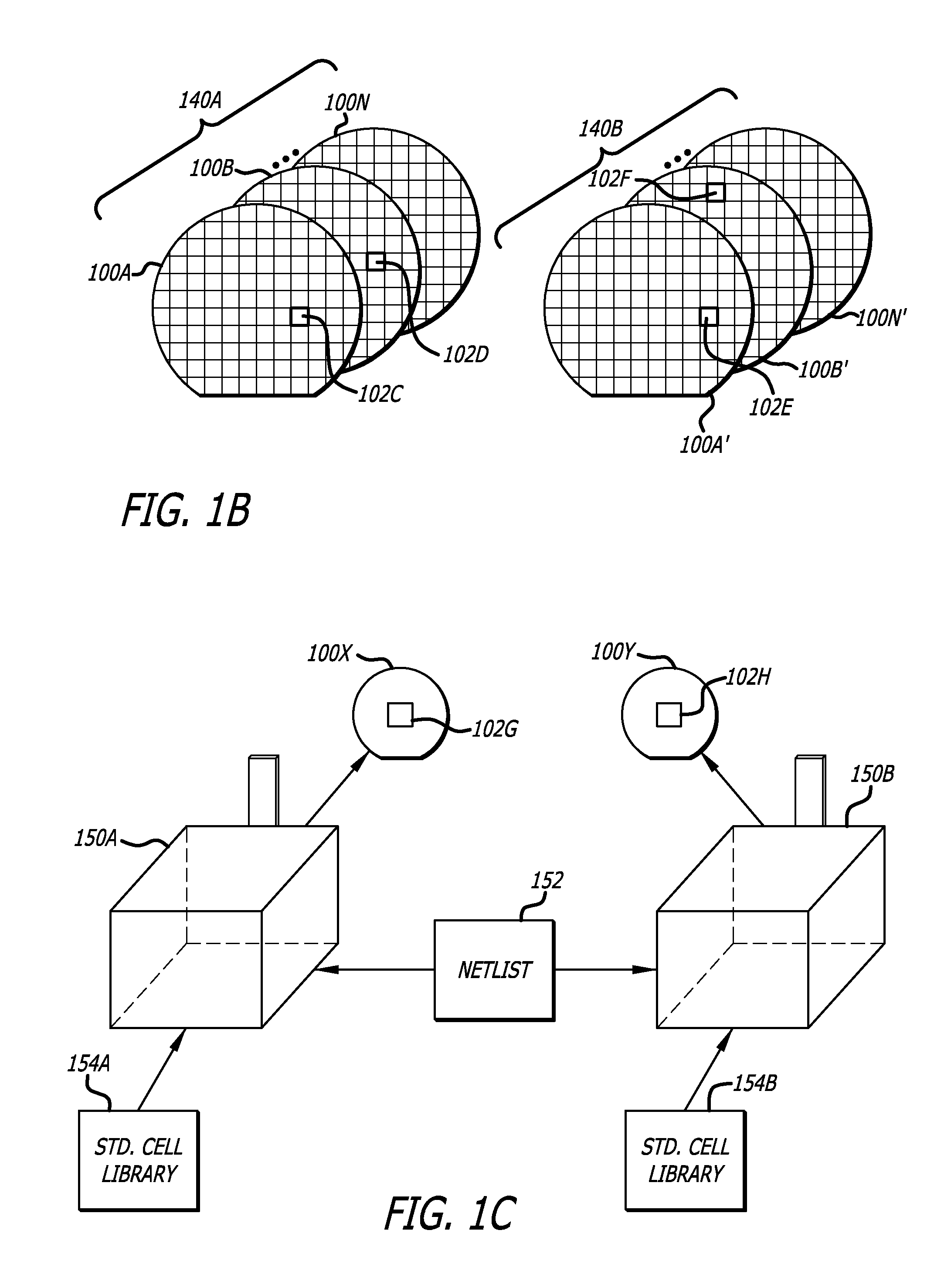
Variations in semiconductor processing of an integrated circuit can cause changes in its performance and yield.

Method used


Image

  • Methods, systems, and apparatus for timing and signal integrity analysis of integrated circuits with semiconductor process variations
  • Methods, systems, and apparatus for timing and signal integrity analysis of integrated circuits with semiconductor process variations
  • Methods, systems, and apparatus for timing and signal integrity analysis of integrated circuits with semiconductor process variations

Examples


Embodiment Construction

[0020]In the following detailed description of the embodiments of the invention, numerous specific details are set forth in order to provide a thorough understanding of the embodiments of the invention. However, it will be obvious to one skilled in the art that the embodiments of the invention may be practiced without these specific details. In other instances well known methods, procedures, components, and circuits have not been described in detail so as not to unnecessarily obscure aspects of the embodiments of the invention.

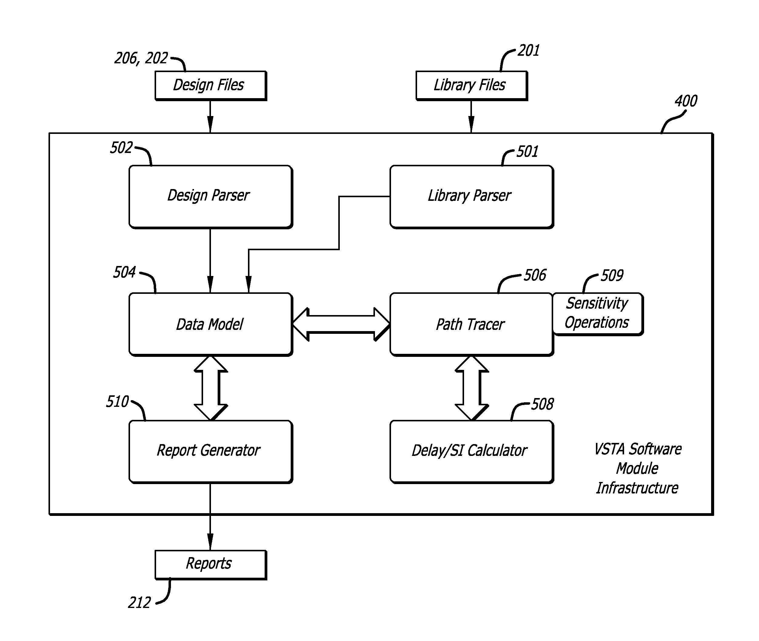
[0021]The embodiments of the invention include a method, apparatus and system for a timing analysis of a physical design of circuits within an integrated circuit chip. In this context, timing analysis also includes considering the effect of crosstalk on the timing of the circuit. In other words, the reference to static timing analysis herein includes a “noise aware static timing analysis”, although the techniques apply equally well to static timing analysis wi...


PUM


Abstract

In one embodiment of the invention, a method of statically analyzing an integrated circuit with process and environment variations is provided. The method includes characterizing each circuit cell of a cell library for a sensitivity to process parameter variations within a predetermined range; creating a timing graph corresponding to a netlist representing an integrated circuit design; along nodes of the timing graph, computing delay values including sensitivities to process variations; for each selected output node of the netlist, propagating a full timing value function with the sensitivities to the selected output nodes; and generating a parameterized timing report including the sensitivities to the process variations.

Description

CROSS-REFERENCE TO RELATED APPLICATIONS[0001]This non-provisional U.S. patent application is a divisional and claims the benefit of U.S. patent application Ser. No. 11 / 560,261 entitled TIMING AND SIGNAL INTEGRITY ANALYSIS OF INTEGRATED CIRCUITS WITH SEMICONDUCTOR PROCESS VARIATIONS” filed on Nov. 15, 2006 by Vinod Kariat et al, now allowed. U.S. patent application Ser. No. 11 / 560,261 claims the benefit of U.S. Provisional Patent Application No. 60 / 737,109 entitled “TIMING AND SIGNAL INTEGRITY ANALYSIS OF INTEGRATED CIRCUITS WITH SEMICONDUCTOR PROCESS VARIATIONS” filed on Nov. 15, 2005 by Vinod Kariat et al.FIELD[0002]The embodiments of the invention relate generally to electronic design automation (EDA) for integrated circuits. More particularly, the embodiments of the invention relate to static timing analysis of integrated circuits with consideration for semiconductor process and environmental variations.BACKGROUND[0003]Designing and manufacturing semiconductor integrated circuits...

Claims


Application Information

Patent Timeline
Patent Type & Authority Patents(United States)
IPC IPC(8): G06F17/50
CPCG06F17/5036G06F30/367
Inventor KARIAT, VINODPHILLIPS, JOEL R.KELLER, IGOR
Owner CADENCE DESIGN SYST INC
Learn More