Multi-chip package with improved signal transmission

a multi-chip, signal-transmission technology, applied in the direction of transformer/inductance details, semiconductor devices, semiconductor/solid-state device details, etc., can solve the problems of signal distortion, difficult to prevent signal interference, and small distance between the respective inductor pads, etc., to achieve the effect of improving the signal transmission speed

Active Publication Date: 2014-01-21
SK HYNIX INC
View PDF11 Cites 0 Cited by
  • Summary
  • Abstract
  • Description
  • Claims
  • Application Information

AI Technical Summary

Benefits of technology

[0010]An MCP capable of improving signal transmission speed between stacked packages is described herein.

Problems solved by technology

However, when the TSVs are used, signal distortion may occur.
However, in the case of the MCP including the inductor pads, the distance between the respective inductor pads is too small.
Therefore, it is difficult to prevent the signal interference, and the resulting distortion, due to adjacent inductor pads.
Furthermore, the signal transmission speed may decrease.

Method used


Image

  • Multi-chip package with improved signal transmission
  • Multi-chip package with improved signal transmission
  • Multi-chip package with improved signal transmission

Examples


Embodiment Construction

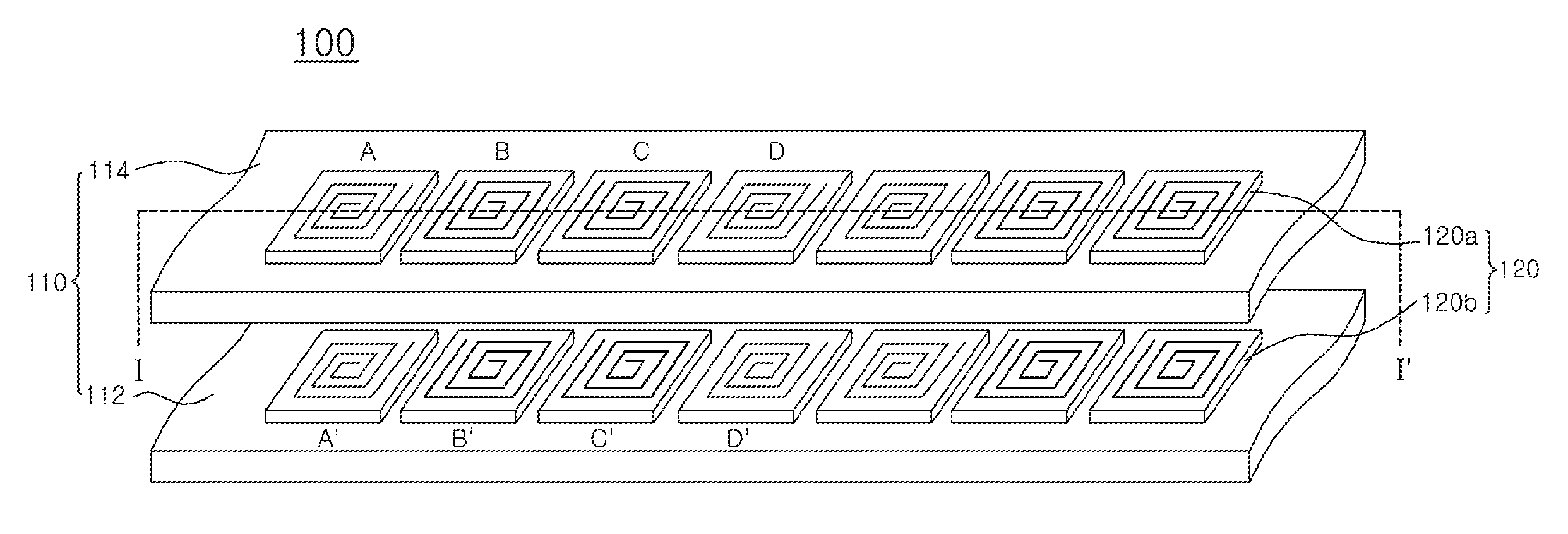
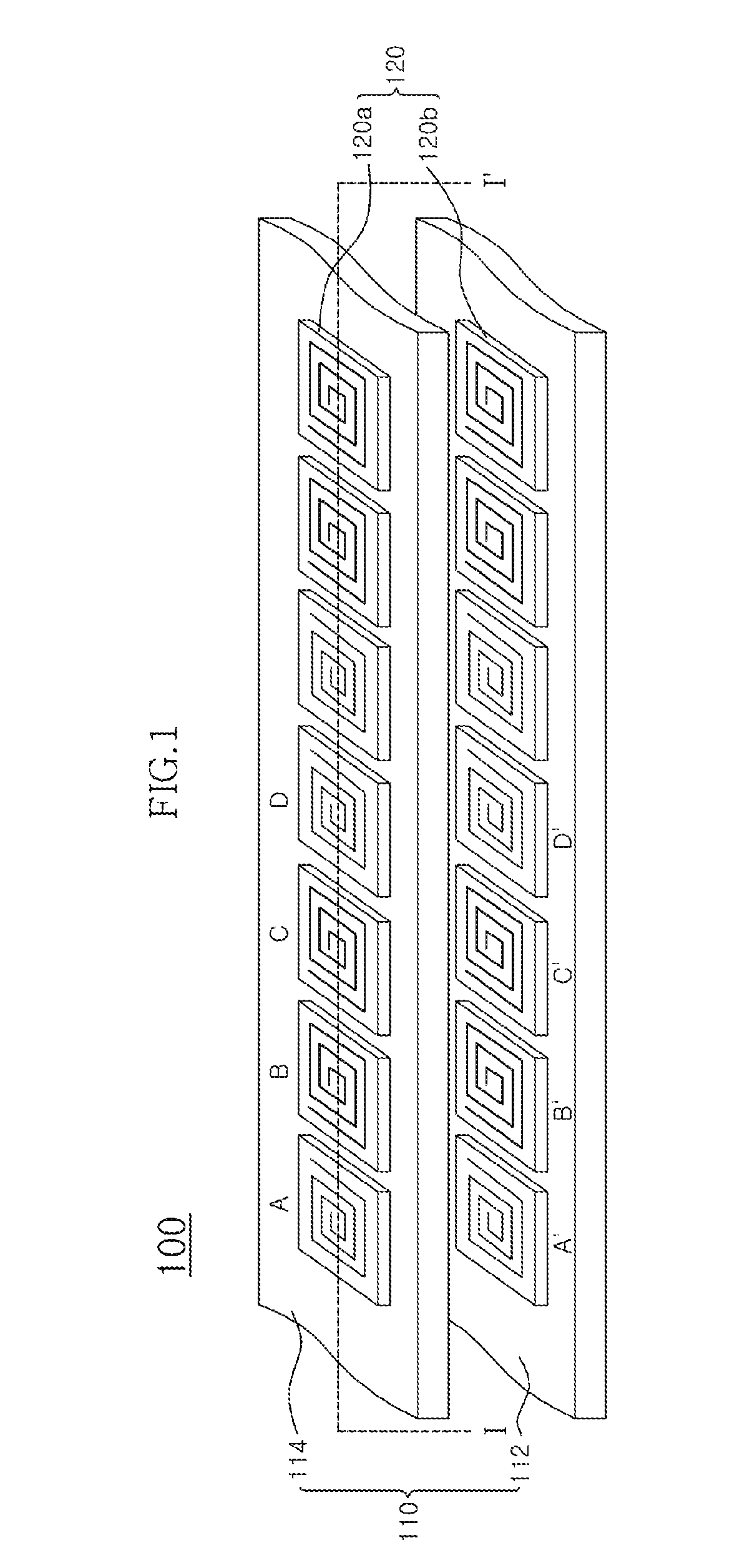
[0020]Hereinafter, a multi-chip package (MCP) according to the present invention will be described below with reference to the accompanying drawings through exemplary embodiments.

[0021]FIG. 1 is a perspective view of an MCP according to one embodiment of the invention. FIG. 2 is a cross-sectional view of the MCP according to an embodiment of the invention.

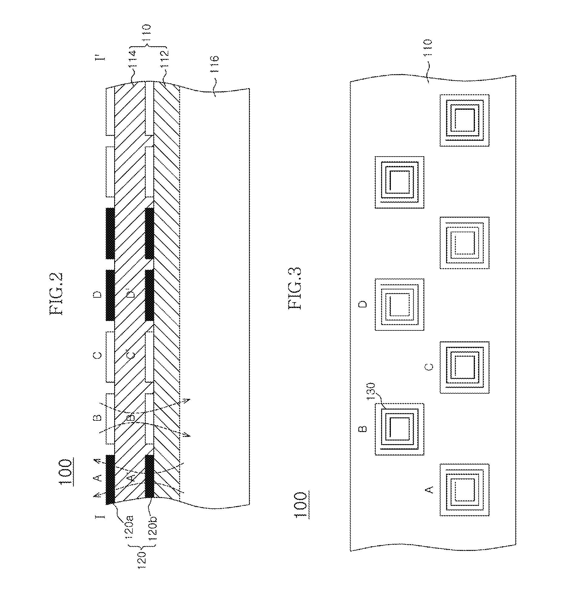
[0022]Referring to FIGS. 1 and 2, the MCP 100 according to the embodiment includes a plurality of chips 110 and a plurality of inductor pads 120.

[0023]The chips 110 include an upper chip 114 and a lower chip 112 which are sequentially stacked on a substrate 116 as illustrated in FIG. 2. The upper chip 114 and the lower chip 116 may be different types of chips or the same type of chips.

[0024]The upper and lower chips 114 and 116 include upper chip and lower chip inductor pads 120a and 120b which are respectively formed at the corresponding positions so as to have the same current and magnetic flux direction.

[0025]On the other hand, ...


PUM


Abstract

Provided is an MCP including a plurality chips stacked therein. Each of the chips includes a plurality of inductor pads configured to transmit power or signals, and at both sides of a reference inductor pad, a first and a second inductor pads are formed to generate magnetic fluxes in different directions from each other.

Description

REFERENCES TO RELATED APPLICATION[0001]The present application claims priority under 35 U.S.C. §119(a) to Korean application number 10-2010-0017458, filed on Feb. 26, 2010, in the Korean Intellectual Property Office, which is incorporated herein by reference in its entirety.BACKGROUND[0002]1. Technical Field[0003]The present invention relates to a semiconductor integrated circuit, and more particularly, to a multi-chip package (MCP).[0004]2. Related Art[0005]An MCP is a package for a plurality of chips, and may be used for combining a memory chip with non-memory chips depending on an application product. MCP contributes to increasing the area efficiency for mobile devices such as a mobile phone.[0006]There are a variety of methods for manufacturing the MCP. For example, in a 3D stacking method, the plurality of chips are vertically stacked, and electrically coupled to each other by through silicon vias (TSVs).[0007]Since the MCP manufactured using the 3D stacking method does not req...

Claims


Application Information

Patent Timeline
Patent Type & Authority Patents(United States)
IPC IPC(8): H01L27/08
CPCH01L23/48H01L25/0657H01L2924/00013H01L2225/06531H01L2924/0002H01L2224/13099H01L2224/13599H01L2224/05599H01L2224/05099H01L2224/29099H01L2224/29599H01L2924/00
Inventor KIM, YOUNG WONLEE, JUN HOKIM, HYUN SEOKJUNG, BOO HOCHO, SUN KIKIM, YANG HEE
Owner SK HYNIX INC
Why Eureka
Try Eureka