Multi-input differential amplifier with dynamic transconductance compensation

a technology of transconductance compensation and differential amplifier, which is applied in differential amplifiers, amplifiers with semiconductor devices/discharge tubes, amplifier details, etc., can solve the problem of cost in chip area, and achieve the effect of increasing the possible interpolation range of input voltage and enhancing output voltage accuracy

Inactive Publication Date: 2014-02-04
NOVATEK MICROELECTRONICS CORP
View PDF2 Cites 78 Cited by
  • Summary
  • Abstract
  • Description
  • Claims
  • Application Information

AI Technical Summary

Benefits of technology

[0009]An amplifier with dynamic transconductance compensation is disclosed, which can enhance output voltage accuracy and increase a possible interpolation range for input voltages.

Problems solved by technology

However, this architecture requires 2^3−1 devices for selection, and is therefore costly in terms of chip area.

Method used


Image

  • Multi-input differential amplifier with dynamic transconductance compensation
  • Multi-input differential amplifier with dynamic transconductance compensation
  • Multi-input differential amplifier with dynamic transconductance compensation

Examples


Embodiment Construction

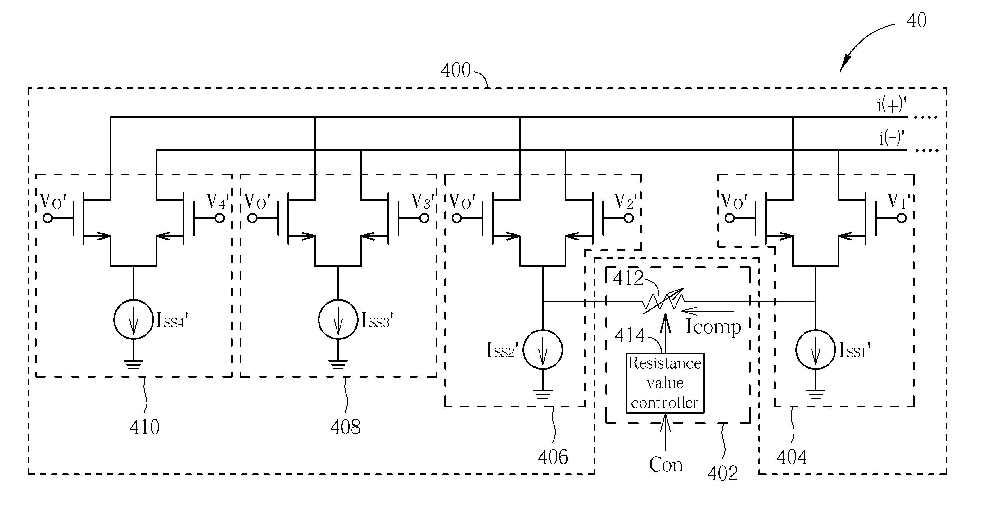
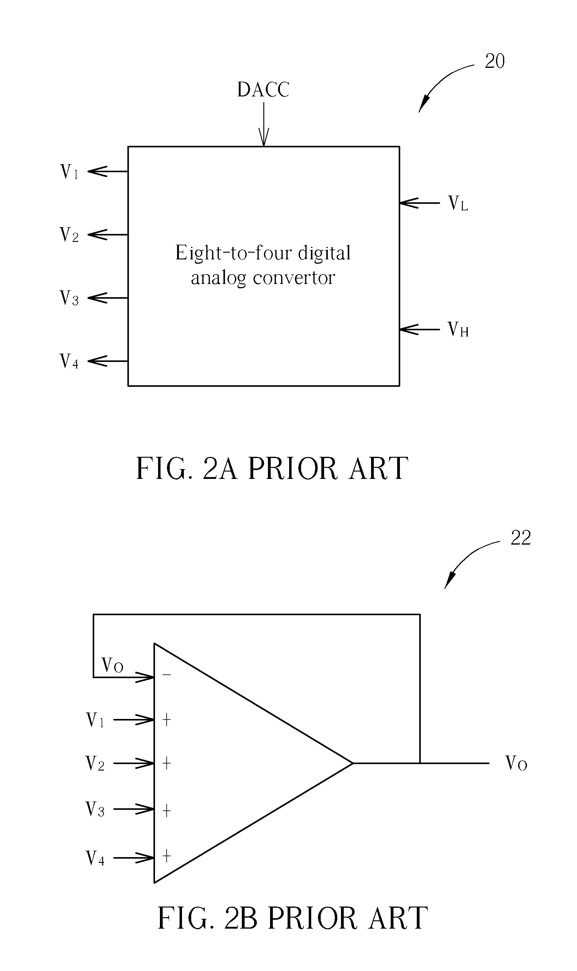
[0025]Please refer to FIG. 3A and FIG. 3B. FIG. 3A is a schematic diagram of differential input pairs 302-308 of an input stage 30 of the multi-input differential amplifier 22 shown in FIG. 2B. FIG. 3B is a schematic diagram of ideal output voltages Vo of the differential input pairs 302-308 corresponding to different combinations of the input voltages V1-V4 and different values of a digital analog conversion code DACC. In FIG. 3A, the multi-input differential amplifier 22 includes the input stage 30, an active load, and an output stage (not shown). As shown in FIG. 3A, the input stage 30 includes four differential input pairs 302-308, and includes reference current sources Iss1-Iss4, respectively, to form a source follower architecture.

[0026]Under this architecture, ideally, as shown in FIG. 3B, it is assumed that the input voltages V1-V4 are composed of a combination of voltage levels VH and VL and that their corresponding transconductance values gm1-gm4 equal the transconductance...


PUM


Abstract

A multi-input differential amplifier with dynamic transconductance compensation is disclosed. The multi-input differential amplifier includes an input stage, an output stage and a transconductance compensation circuit. The input stage includes a plurality of differential input pairs, which includes a first differential input pair, a second differential input pair, a third differential input pair and a fourth differential input pair, for generating a pair of differential signals according to a first input signal, a second input signal, a third input signal, a fourth input signal, and an output signal. The output stage is utilized to generate the output signal in response to the pair of differential signals. The transconductance compensation circuit is coupled between the first and the second differential input pair, for compensating a first transconductance of the first differential input pair and a second transconductance of the second differential input pair.

Description

BACKGROUND OF THE INVENTION[0001]1. Field of the Invention[0002]The present invention relates to a multi-input differential amplifier, and more specifically, to a multi-input differential amplifier capable of performing dynamic transconductance compensation to enhance output voltage accuracy and increase input voltage interpolation range.[0003]2. Description of the Prior Art[0004]Generally, to reduce chip area, a multi-bit output buffer of a driving chip usually utilizes multi-input-pair interpolation amplifiers, which operate by inputting input voltage values with different weighting, and then generating a combined output voltage via interpolation.[0005]For example, please refer to FIG. 1, which is a schematic diagram of a conventional eight-to-one digital analog convertor (DAC) 10. As shown in FIG. 1, the eight-to-one DAC 10 selects a suitable voltage to output from eight input voltages, according to a received 3-bit digital analog conversion code DACC. However, this architecture ...

Claims


Application Information

Patent Timeline
Patent Type & Authority Patents(United States)
IPC IPC(8): H03F3/45
CPCH03F3/45183H03F1/3211
Inventor CHIU, MAO-CHENGCHO, CHUN-YUNG
Owner NOVATEK MICROELECTRONICS CORP
Why Eureka
Try Eureka