System for inspecting surface defects of a specimen and a method thereof

a technology for specimens and inspection systems, applied in the field of systems for inspecting specimen surface defects, can solve the problems of increasing the cost of bf systems with the amount of accessories, increasing the cost of manufacturing processes, and affecting the inspection speed of specimens, so as to increase the inspection speed, reduce the cost, and increase the inspection zone

Inactive Publication Date: 2014-02-04
MFC SEALING TECH
View PDF11 Cites 14 Cited by
  • Summary
  • Abstract
  • Description
  • Claims
  • Application Information

AI Technical Summary

Benefits of technology

[0006]Therefore, it is a primary objective of the present invention to provide an inspection system for inspecting the surface defects of the specimen and an inspection method thereof to achieve the effect of reducing the inspection cost, increasing the inspection speed and calculating the real size of each defect on a specimen surface.
[0024]Preferably, the step of using a platform may further include using a drive module connected to the laser module and the image pick-up module to drive the laser module and the image pick-up module to move simultaneously, and causes the laser beam to irradiate on the surface of the specimen in a straight way.
[0025]The inspection system and method for inspecting the surface defects of a specimen according to the present invention can calculate the real size of each defect on the surface of the specimen by analyzing the intensity of the scattered light or the diameter of the caustic curves captured by the reflected light capture module, so that the present invention has the following advantages.
[0026]Since the inspection system and method of the present invention do not need a high magnification object lens and a high resolution image sensor for acquiring the image of micro-level defects or particles, the present invention can increase the inspection speed because of the larger inspection zone and decrease the cost because the present invention only need to get the diameter of the caustic curves from the reflected light image or the intensity of the scattered light to calculate the size of each defect by using the process module.

Problems solved by technology

Therefore, inspecting the defects of the wafer surface becomes a significant issue in the chip manufacture process for increasing the yield rate and decreasing the cost of manufacturing process.
Hence the cost of BF system will increase with the amount of its accessories, and its inspection speed becomes very slow due to the smaller inspection area.
However, the DF system cannot get the real size of particles on the wafer surface, so it only can be applied to the inspection of bare wafer.

Method used


Image

  • System for inspecting surface defects of a specimen and a method thereof
  • System for inspecting surface defects of a specimen and a method thereof
  • System for inspecting surface defects of a specimen and a method thereof

Examples


Embodiment Construction

[0037]The technical content of the present invention will become apparent by the detailed description of the following embodiments and the illustration of related drawings as follows.

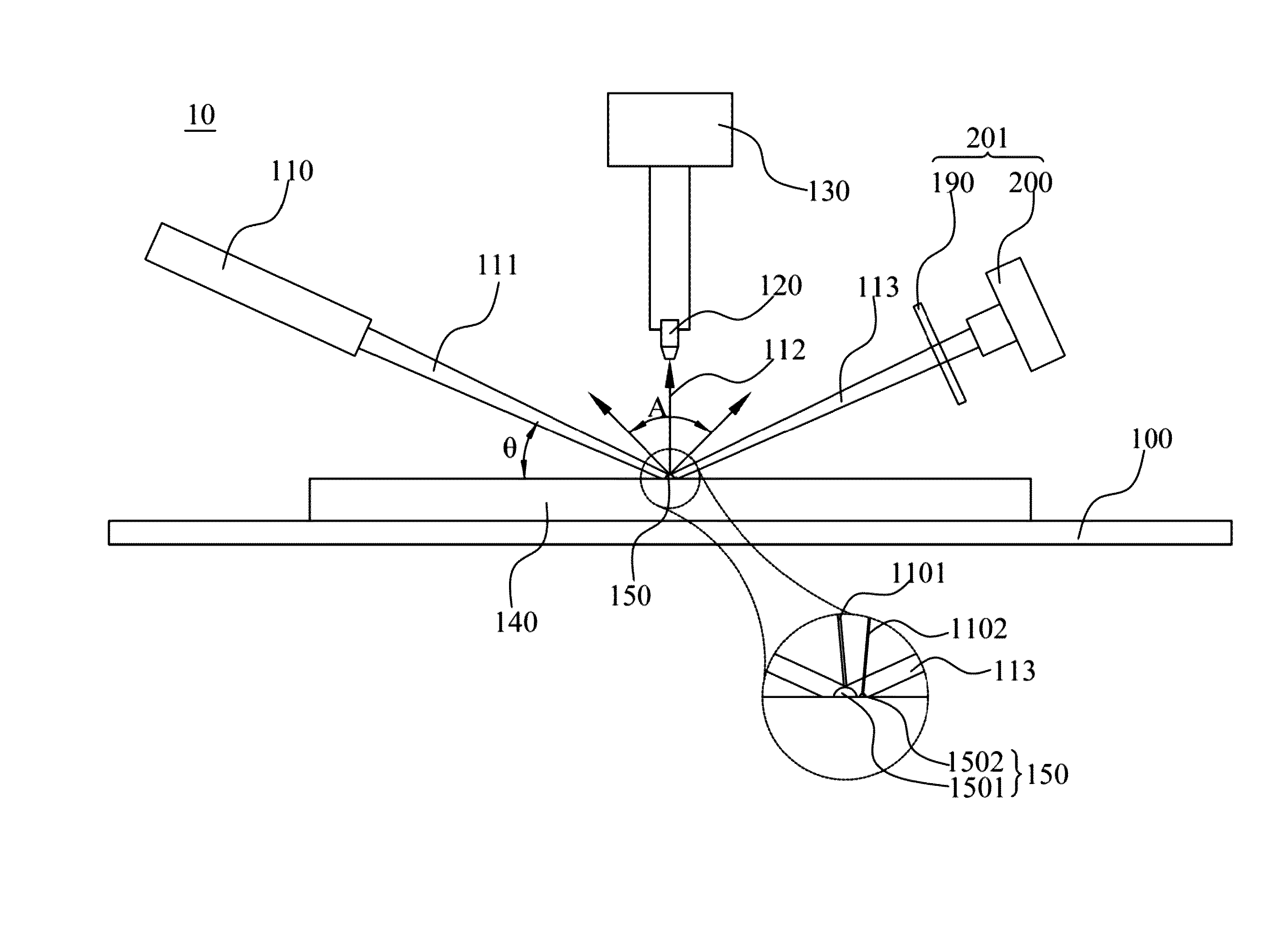
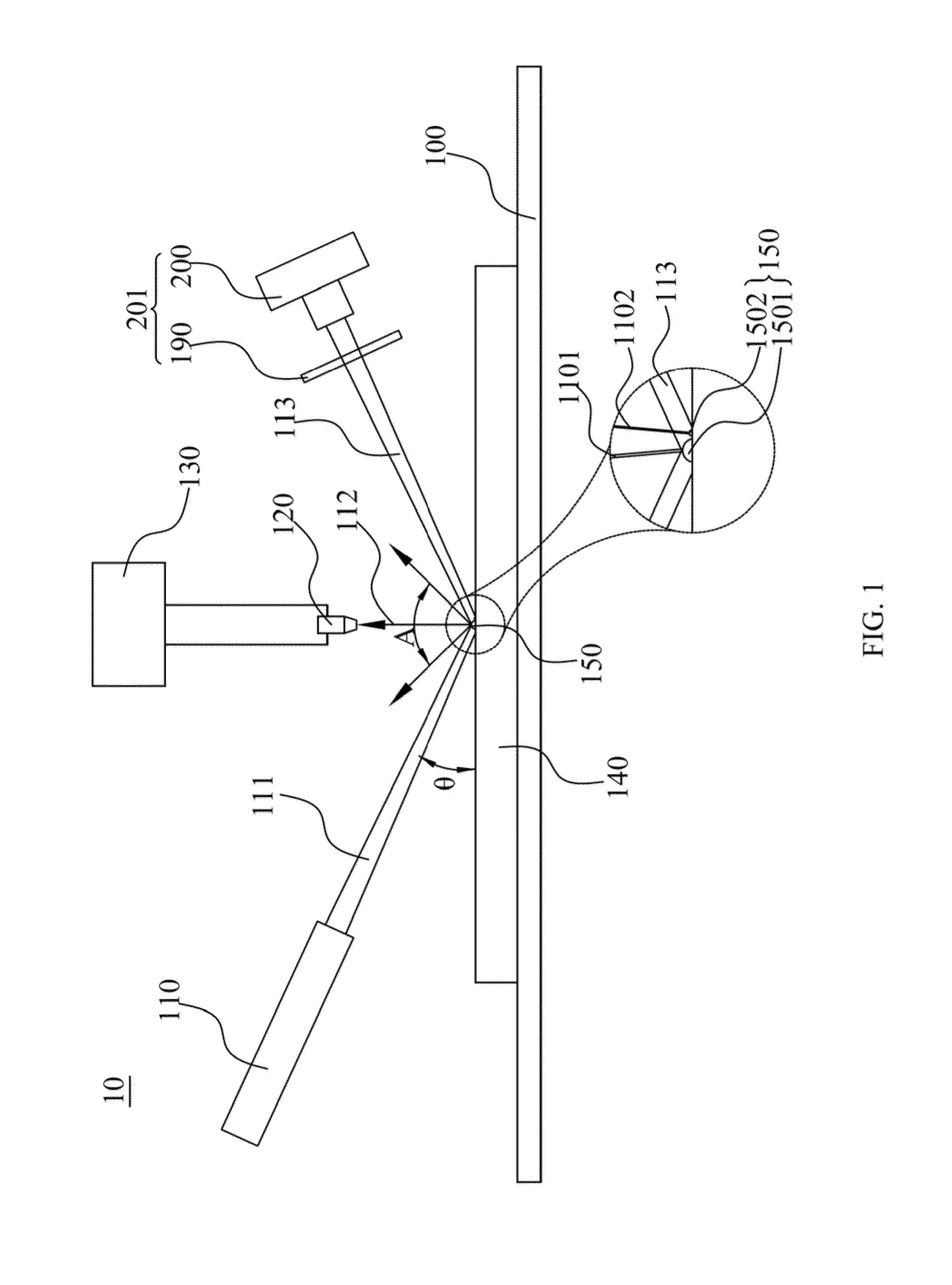
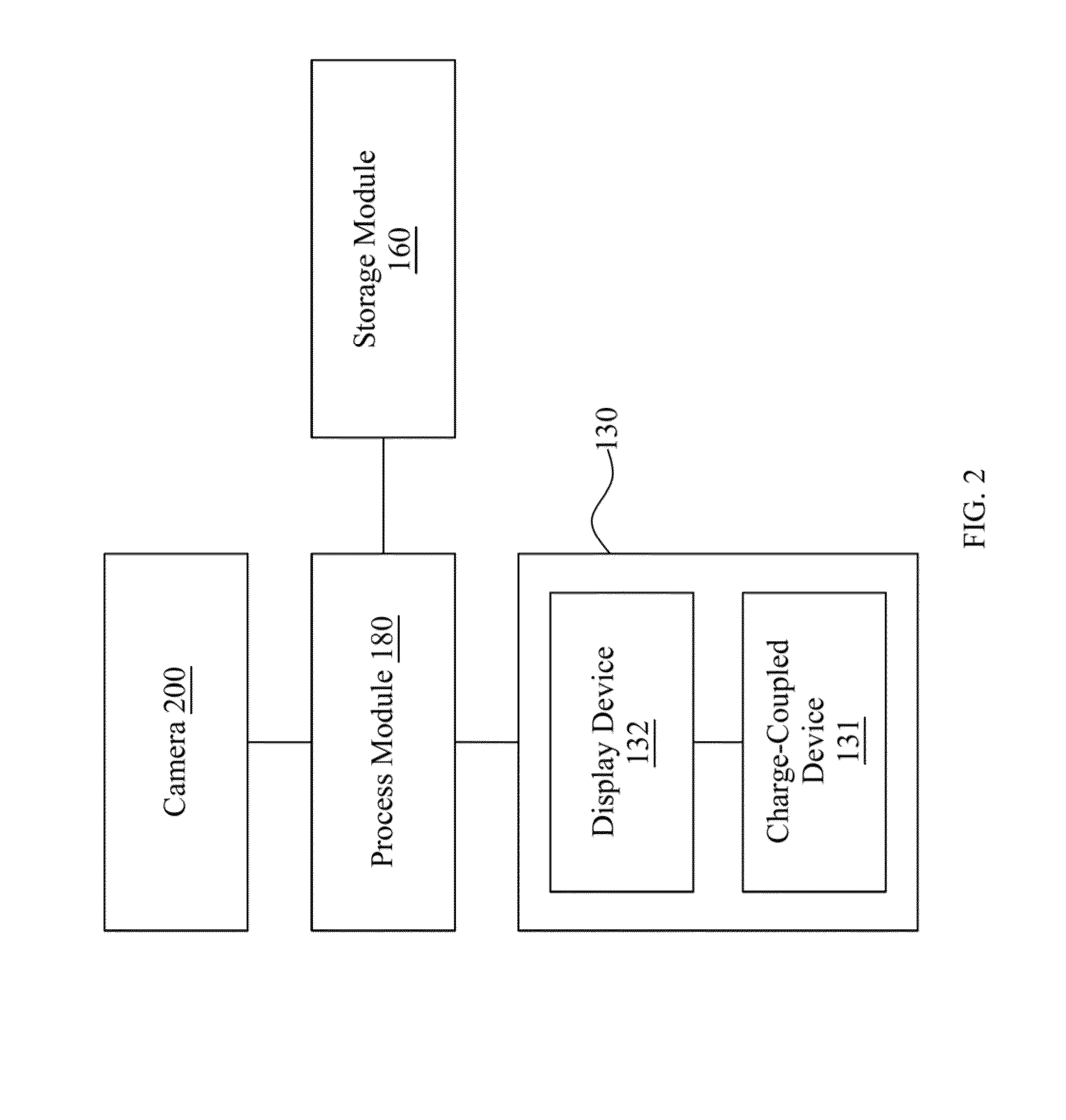
[0038]With reference to FIG. 1 for a schematic view of an embodiment of an inspection system according to the present invention, the inspection system 10 is applied to inspect the surface defects of a specimen. The inspect system 10 includes a platform 100, a laser focus module 110, a microscope objective module 120, an image pick-up module 130, reflected light capture module 201 and a process module 180 (shown in FIG. 2), wherein the platform 100 is used to hold up the specimen.

[0039]The specimen of the present embodiment is a silicon wafer 140, but is not limited thereto. In other embodiments of the present invention, the specimen can be a workpiece or an article and the inspection system 10 of the present invention can detect particles, motes, roughness and the like on a surface of the workpiece or t...


PUM

PropertyMeasurementUnit
angleaaaaaaaaaa
angleaaaaaaaaaa
angleaaaaaaaaaa

Abstract

An inspection system and method for inspecting the surface defects of the specimen is provided. The inspection system includes a laser focus module, a microscope objective module, an image pick-up module, and a process module. The laser focus module configured to emit laser beam on the specimen by a predetermined angle relative to a surface of the specimen, and to generate scattered light and reflected light when the laser beam irradiates on the surface defects of the specimen. The process module can calculate the real size of the defects by using the intensity information obtained from the image pick-up module and the microscope objective module or using the diameter information obtained from the reflected light image while the reflected light projects on a screen.

Description

BACKGROUND OF THE INVENTION[0001]1. Field of the Invention[0002]The present invention generally relates to a system for inspecting surface defects of a specimen and a method thereof, in particular to a system and a method for inspecting the surface defects of the wafer by using the scattered light.[0003]2. Description of the Related Art[0004]In field of semiconductor industry, it is important for the silicon substrate surface to be clean because the defects attached on the surface of the wafer will have great influence upon the chip manufacture process, such as the short circuit phenomenon. Therefore, inspecting the defects of the wafer surface becomes a significant issue in the chip manufacture process for increasing the yield rate and decreasing the cost of manufacturing process.[0005]The wafer inspection systems which are used to detect surface defects on the silicon wafer can be divided into two types, the bright field (BF) system and the dark field (DF) system. In the BF system...

Claims


Application Information

Patent Timeline
Patent Type & Authority Patents(United States)
IPC IPC(8): G01N21/00
CPCG01N21/9501G01N21/00
Inventor HUNG, MIN-WEITSAI, HSIN-YIHUANG, KUO-CHENGHUANG, CHUN-YAO
Owner MFC SEALING TECH
Why Eureka
Try Eureka