Scalable, high-throughput, multi-chamber epitaxial reactor for silicon deposition

a multi-chamber, epitaxial reactor technology, applied in the direction of chemically reactive gases, solid-state diffusion coatings, crystal growth processes, etc., can solve the problems of high cost of producing crystalline-si-wafer-based solar cells, bottleneck in the supply of crystalline-si-wafers, and the need for cleaner, cheaper alternative energy sources. to achieve uniform material deposition

Active Publication Date: 2014-02-18
TESLA INC
View PDF8 Cites 5 Cited by
  • Summary
  • Abstract
  • Description
  • Claims
  • Application Information

AI Technical Summary

Benefits of technology

[0015]One embodiment of the present invention provides a system for material deposition. The system includes an AC (alternating current) panel for providing electrical power to the system, a susceptor load / unload station, a running beam coupled to the load / unload station for loading / unloading susceptors, and a multi-chamber module. The multi-chamber module includes a gas box, an SCR panel, and a number of reaction chambers situated next to each other. The reaction chamber is formed using a material that is transparent to radiation energy, a pair of susceptors situated inside the reaction chamber. Each susceptor has a front side and a back side, and the front side mounts a number of substrates. The susceptors are positioned vertically in such a way that the front sides of the susceptors face each other, and the vertical edges of the susceptors are in contact with each other, thereby forming a substantially enclosed narrow channel between the substrates mounted on different susceptors. The system also includes a number of gas nozzles. At least one of the gas nozzles includes a gas inlet for injecting reaction gas into the narrow channel and a gas outlet for outputting exhaust. The gas inlet and the gas outlet are coupled to different gas lines, and the gas inlet and the gas outlet are controlled in such a way that reaction gas flow directions inside the narrow channel can be alternated, thereby facilitating uniform material deposition. In addition, the system includes a number of heating units situated outside the reaction chamber. At least one heating unit is situated between the side walls of two adjacent reaction chambers, thereby allowing the at least one heating unit to heat the two adjacent reaction chambers simultaneously. In addition, the heating units are arranged in such a way that they radiate heat energy directly to the back side of the susceptors.
[0019]In a variation on the embodiment, the gas inlet is configured to inject a small amount of purge gas when the gas inlet is not injecting reaction gas to the narrow channel during material deposition, thereby preventing material deposition around the gas inlet.

Problems solved by technology

The negative environmental impact caused by the use of fossil fuels and their rising cost have resulted in a dire need for cleaner, cheaper alternative energy sources.
However, the cost of producing crystalline-Si-wafer based solar cell is high, and the waste of Si material in the processes of ingot-cutting and wafer-polishing has caused a bottleneck in the supply of crystalline-Si wafers.
However, there is a lack of suitable Si epitaxy tools that can meet the demand for high throughput and low deposition cost for Si film layers with thickness up to several tens of microns, as required by the solar cell industry.
Although these epitaxial tools can deliver Si films with the highest quality, these tools are not compatible, in terms of throughput and gas conversion efficiency, with the economics of the solar cell industry.
Although barrel reactor 200 can batch process multiple wafers, the number of wafers it can process is limited by the architect of the system, the size of the chamber, and the design of the susceptor.
Once built, it is difficult to modify the reactor or the susceptor to accommodate more wafers.
However, it does not solve the issues of low throughput, low reaction gas conversion rate, low power utilization efficiency, minimal Si deposition on the quartz chamber, and processing scalability.
In addition, using the same gas lines for gas inlet and outlet increased the risk of contamination and re-deposition.

Method used


Image

  • Scalable, high-throughput, multi-chamber epitaxial reactor for silicon deposition
  • Scalable, high-throughput, multi-chamber epitaxial reactor for silicon deposition
  • Scalable, high-throughput, multi-chamber epitaxial reactor for silicon deposition

Examples


Embodiment Construction

[0038]The following description is presented to enable any person skilled in the art to make and use the embodiments, and is provided in the context of a particular application and its requirements. Various modifications to the disclosed embodiments will be readily apparent to those skilled in the art, and the general principles defined herein may be applied to other embodiments and applications without departing from the spirit and scope of the present disclosure. Thus, the present invention is not limited to the embodiments shown, but is to be accorded the widest scope consistent with the principles and features disclosed herein.

Overview

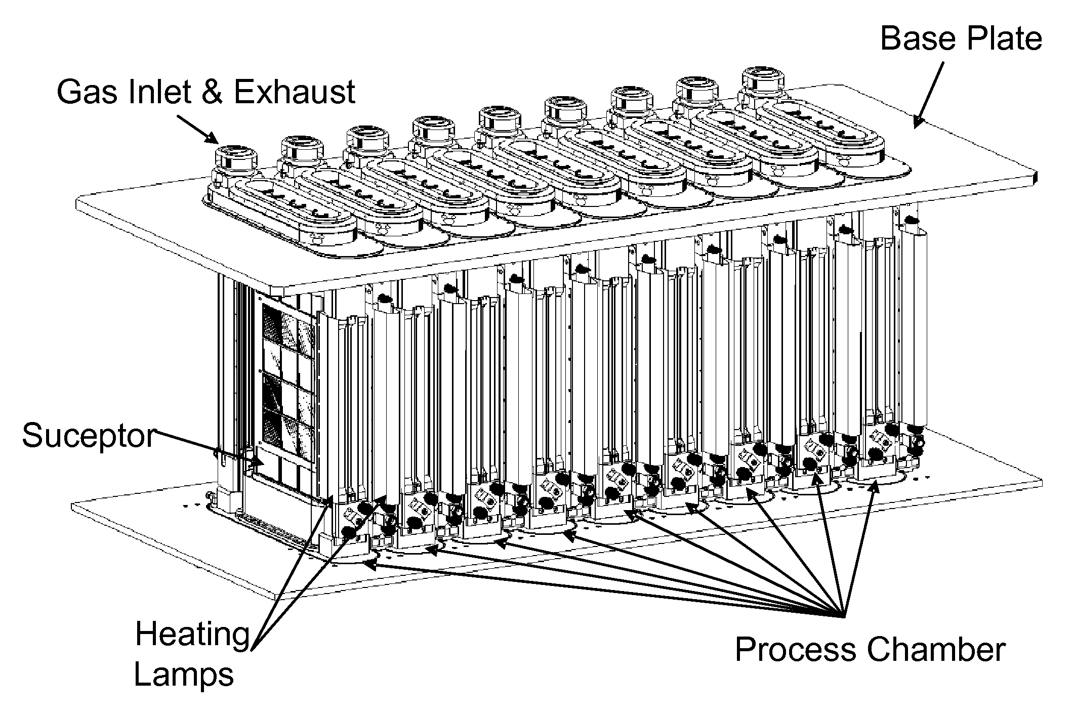
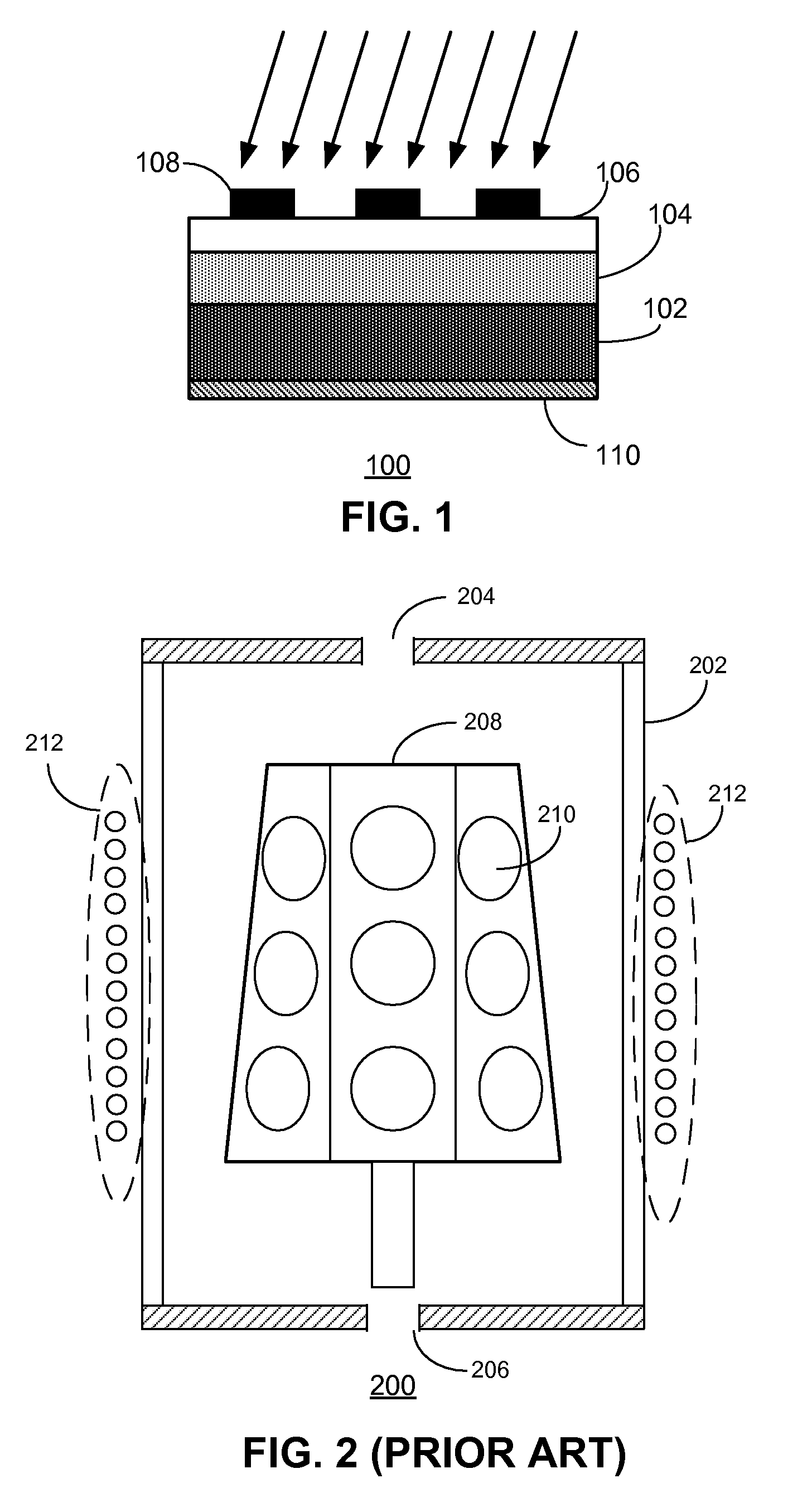
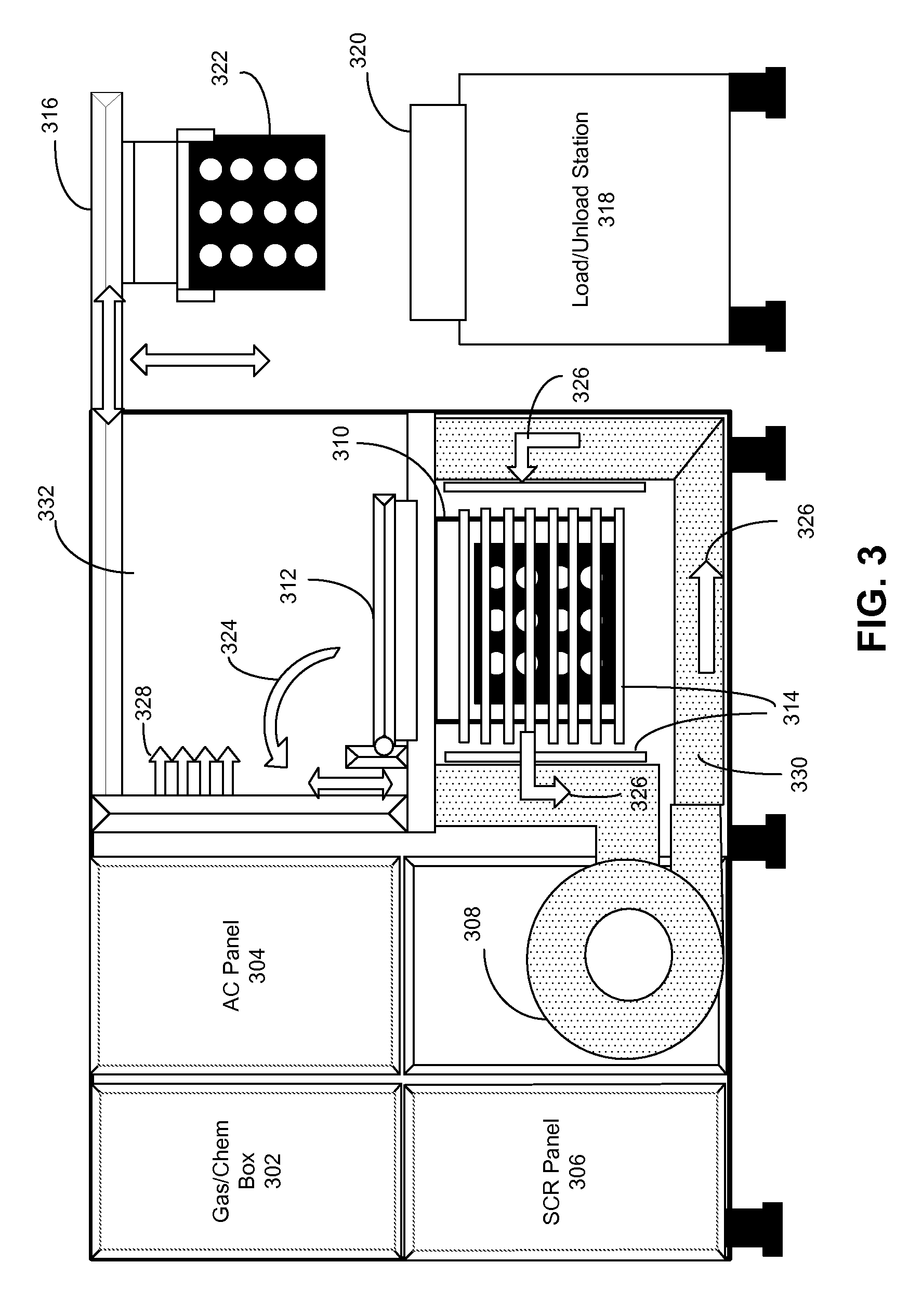
[0039]Embodiments of the present invention provide a scalable, high-throughput multi-chamber epitaxial reactor for Si deposition. The reactor includes a number of extendible, independently controlled multi-chamber modules. The reaction chambers are heated by lamp heating units which are alternately inserted between adjacent chambers. Each reaction ...


PUM

PropertyMeasurementUnit
widthaaaaaaaaaa
widthaaaaaaaaaa
widthaaaaaaaaaa

Abstract

One embodiment provides an apparatus for material deposition. The apparatus includes a reaction chamber, and a pair of susceptors. Each susceptor has a front side and a back side, and the front side mounts substrates. The susceptors are positioned vertically in such a way that the front sides of the susceptors face each other, and the vertical edges of the susceptors are in contact with each other, thereby forming a substantially enclosed narrow channel between the substrates. The apparatus also includes a number of gas nozzles for injecting reaction gases. The gas nozzles are controlled in such a way that gas flow directions inside the chamber can be alternated, thereby facilitating uniform material deposition. The apparatus includes a number of heating units situated outside the reaction chamber. The heating units are arranged in such a way that they radiate heat energy directly to the back sides of the susceptors.

Description

RELATED APPLICATION[0001]This application claims the benefit of U.S. Provisional Application No. 61 / 104,166, entitled “Scalable, High Throughput, Multi-chamber CVD Reactor for Silicon Deposition” by inventors Steve Poppe, Yan Rozenzon, David Z. Chen, Xiaole Yan, Peijun Ding, and Zheng Xu, filed 9 Oct. 2008.BACKGROUND[0002]1. Field[0003]This disclosure is generally related to silicon deposition. More specifically, this disclosure is related to a scalable, high throughput multi-chamber batch type epitaxial reactor for silicon deposition.[0004]2. Related Art[0005]The negative environmental impact caused by the use of fossil fuels and their rising cost have resulted in a dire need for cleaner, cheaper alternative energy sources. Among different forms of alternative energy sources, solar power has been favored for its cleanness and wide availability.[0006]A solar cell converts light into electricity using the photoelectric effect. There are several basic solar cell structures, including ...

Claims


Application Information

Patent Timeline
Patent Type & Authority Patents(United States)
IPC IPC(8): C23C16/00
CPCC23C16/4587C23C16/45502C23C16/46C30B25/165C30B25/105C30B25/12C23C16/54
Inventor POPPE, STEVEROZENZON, YANCHEN, DAVID Z.YAN, XIAOLEDING, PEIJUNXU, ZHENG
Owner TESLA INC
Why Eureka
Try Eureka