

Methods and structure for adapting MEMS structures to form electrical interconnections for integrated circuits
- Summary
- Abstract
- Description
- Claims
- Application Information
AI Technical Summary
Benefits of technology
Problems solved by technology
Method used
Image

Examples
Embodiment Construction
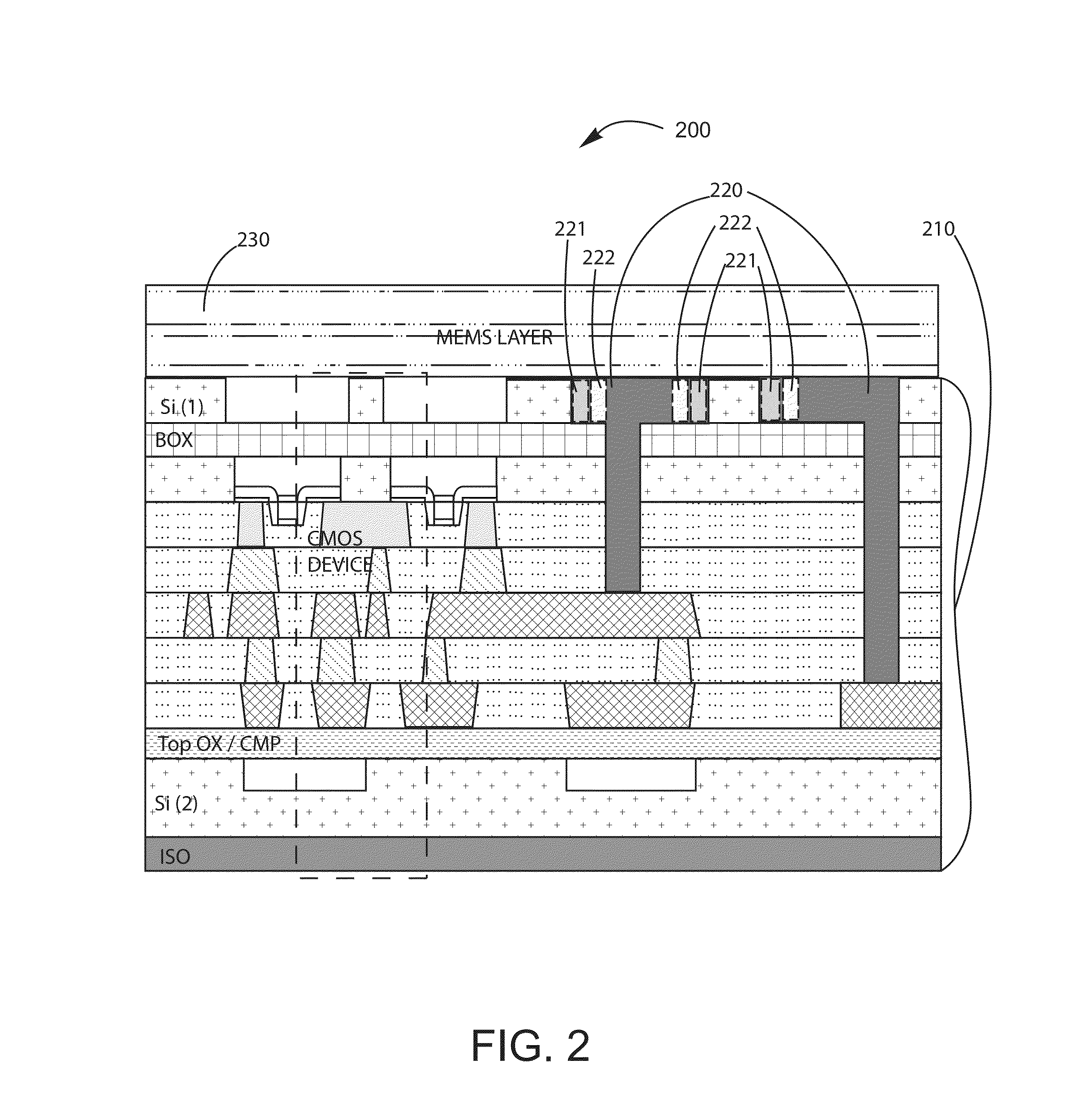
[0022]According to the present invention, techniques related generally to integrated devices and systems are provided. More particularly, the present invention provides a methods and structure for adapting MEMS structures to form electrical interconnections for integrated circuits (ICs). Merely by way of example, the MEMS devices can include at least an accelerometer, a pressure sensor, a gyroscope, a microphone, an inertial sensor, and others. Additionally, the other applications include at least a sensor application or applications, system applications, and broadband applications, among others. But it will be recognized that the invention has a much broader range of applicability.
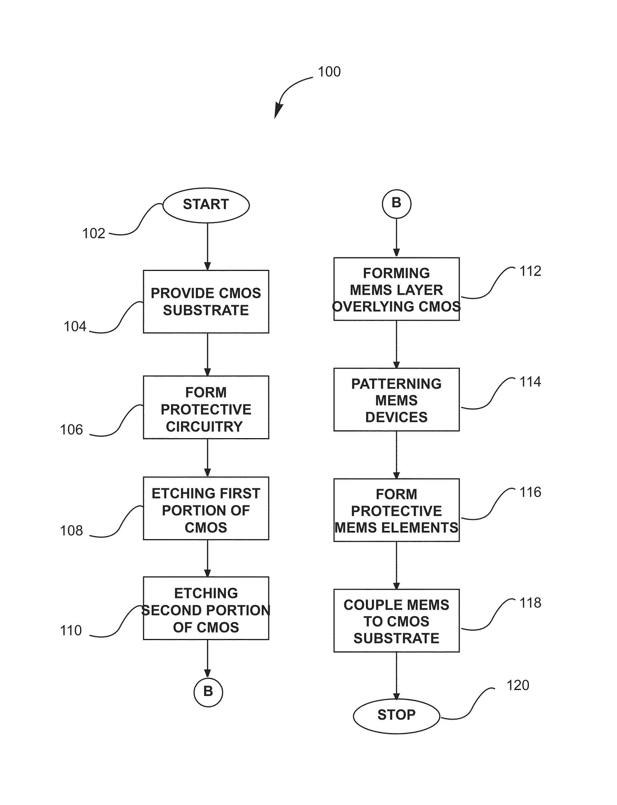
[0023]FIG. 1 is a simplified flow diagram illustrating methods of fabricating an inertial sensor using tilt conversion according to an embodiment of the present invention.
[0024]As shown in FIG. 1, embodiments of a manufacturing process are illustrated. Various steps are also outlined below.[0025]1. Start;...
PUM
 Abstract
Description
Claims
Application Information