Liquid crystal display device, manufacturing method and repair method thereof

a liquid crystal display and manufacturing method technology, applied in optics, instruments, electrical devices, etc., can solve the problems of reducing the image quality of the lcd device, prone to electrostatic damage, and so as to reduce the disadvantageous effect of image quality after repairing, the effect of reducing the probability of electrostatic damag

Active Publication Date: 2014-02-18
BEIJING BOE OPTOELECTRONCIS TECH CO LTD
View PDF17 Cites 2 Cited by
  • Summary
  • Abstract
  • Description
  • Claims
  • Application Information

AI Technical Summary

Benefits of technology

[0038]1. The area of the intersection region can be reduced so as to effectively reduce probability of electrostatic break-down.
[0006]The conventional LCD device is prone to electrostatic breakdown and an open is formed in the common electrode after repairing, which degrades image quality of the LCD device. In view of the problems, in an embodiment of the present invention, there is provided a novel LCD device with an electrostatic dissipation path design to reduce probability of electrostatic breakdown, the LCD device can be repaired for many times when electrostatic breakdown occurs, and also disadvantageous effect on the image quality after repairing is reduced. The LCD device is, e.g., a thin film transistor LCD (TFT LCD).
[0041]4. The overlapping area of the intersection region is reduced in structure design, which reduces the induced capacitance between the data signal line and influence on the delay in the data signal line.

Problems solved by technology

The conventional LCD device is prone to electrostatic breakdown and an open is formed in the common electrode after repairing, which degrades image quality of the LCD device.

Method used


Image

  • Liquid crystal display device, manufacturing method and repair method thereof
  • Liquid crystal display device, manufacturing method and repair method thereof
  • Liquid crystal display device, manufacturing method and repair method thereof

Examples


Embodiment Construction

[0026]The exemplary embodiments according to the present invention will be described in detail with reference to the accompanying drawings. This invention may, however, be embodied in many different forms and should not be construed as limited to the embodiments set forth herein. In the context, it will be understood that when an element or layer is referred to as being “on” or “connected to” another element or layer, it can be directly on or connected to the other element or layer, or an intervening element or layer may be present therebetween. Hereinafter, for simplicity, the parts in the present invention corresponding to those in the related art share the same reference numeral.

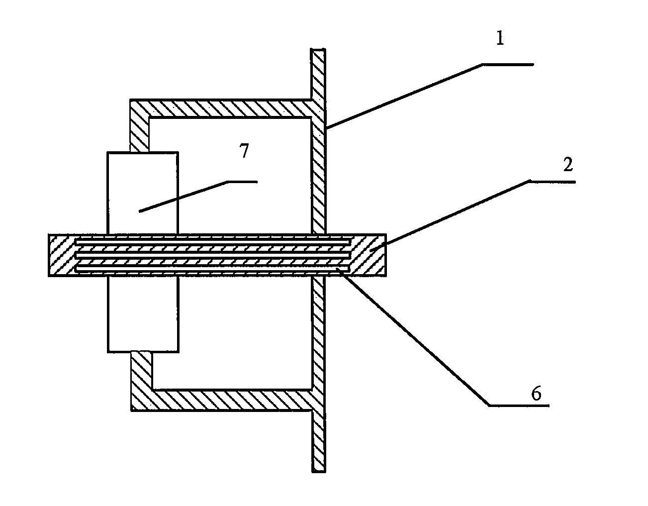
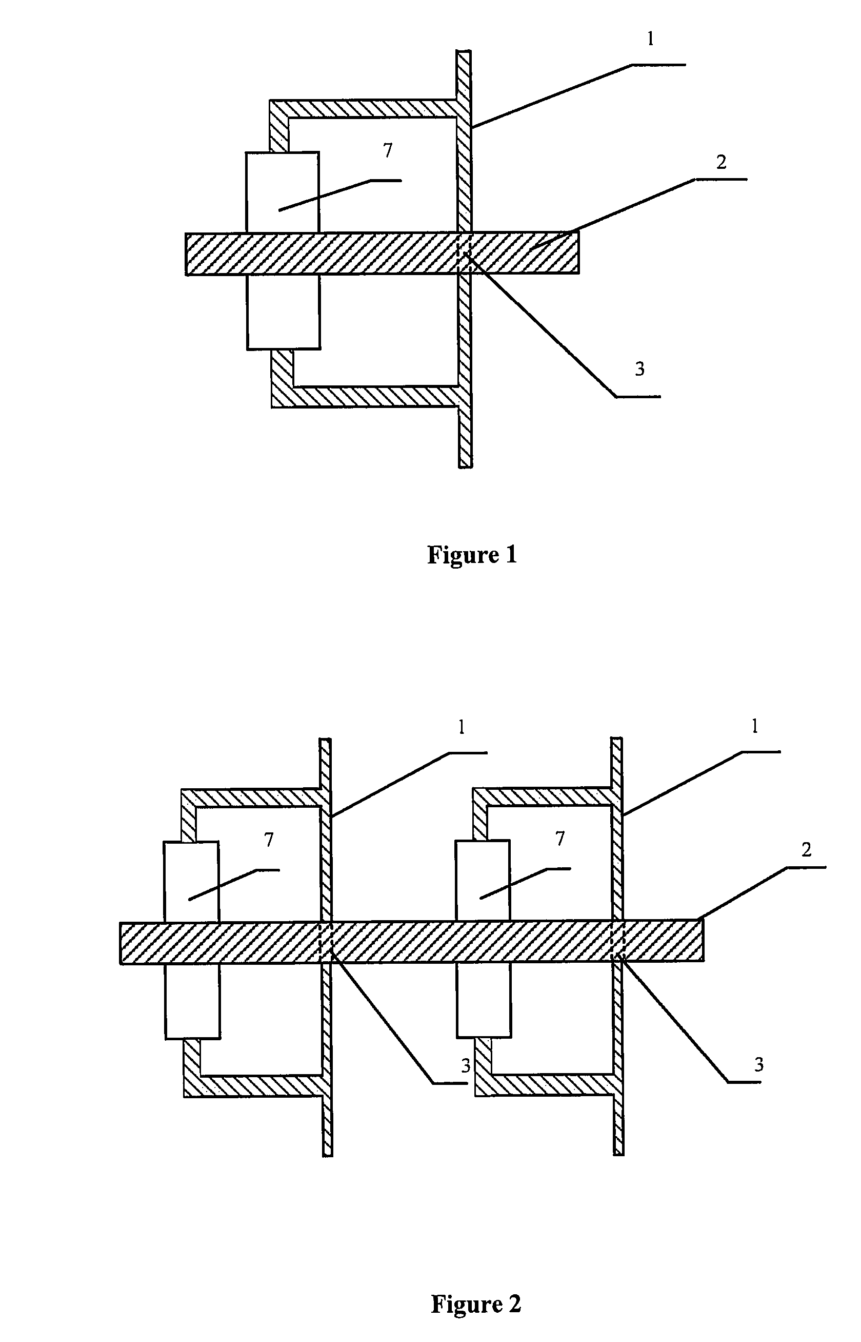
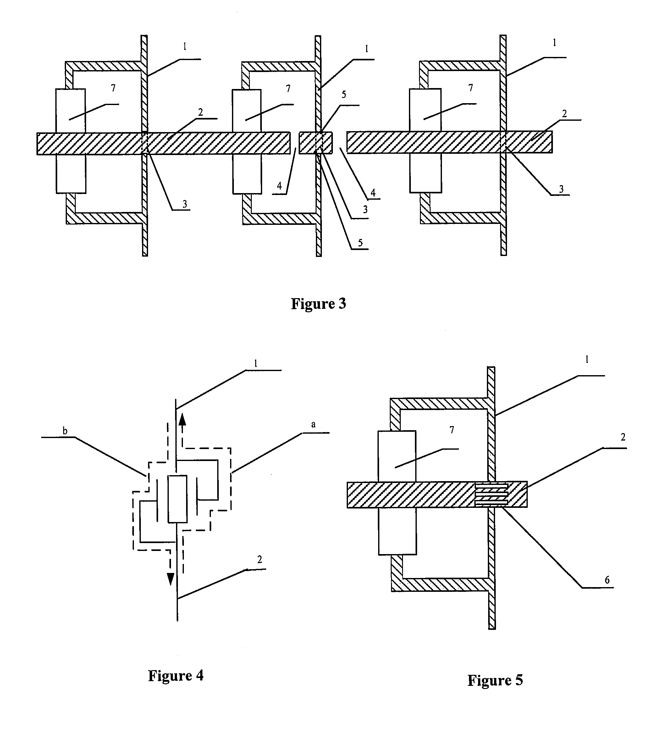
[0027]A liquid crystal display (LCD) device such as a thin film transistor liquid crystal display (TFT LCD) device can be realized by the standard semiconductor processes. As shown in FIG. 4, an antistatic protection circuit 7 (also called an electrostatic short-circuit ring) is formed by connecting two t...


PUM


Abstract

A liquid crystal display (LCD) device is provided. The LCD device comprises a data signal line in a first plane and a common electrode line in a second plane, and the common electrode line comprises an intersection region, which is a region where a projection of the common electrode line in the first plane overlaps with a region of the data signal line. The intersection region comprises a plurality of narrow common electrode lines.

Description

[0001]The present application claims the priority of the Chinese applications No. 200710065589.3 filed in the Chinese Intellectual Property Office on Apr. 17, 2007, the disclosure of which is incorporated herewith by reference.BACKGROUND OF THE INVENTION[0002]The present invention relates to a liquid crystal display (LCD) device, a manufacturing method and a repair method thereof.[0003]During mass production of the current thin film transistor liquid crystal display (TFT LCD), since the activities like transfer of substrates, contact of equipments, and contact of operators may potentially induce electrostatic (ES) that causes an ES voltage. The ES voltage may induce discharge in a short time and produce current substantially larger than the capability of the active devices within the LCD device, i.e., the external ES is transited to the active devices within the LCD device through the data signal lines and results in breakdown. In a conventional wiring design in the TFT array substr...

Claims


Application Information

Patent Timeline
Patent Type & Authority Patents(United States)
IPC IPC(8): G09G3/36
CPCG09G2330/08G09G3/3611G02F1/136204G02F1/133G02F1/13
Inventor GAO, WENBAO
Owner BEIJING BOE OPTOELECTRONCIS TECH CO LTD
Why Eureka
Try Eureka