
Carbon nanotube-based neural networks and methods of making and using same

a carbon nanotube and neural network technology, applied in the field of carbon nanotube switches and methods of making same, can solve the problems of electronics approaching quantum-mechanical boundaries, wiring complexity increasing, and fet complexity increasing

Active Publication Date: 2014-02-25
NANTERO
View PDF48 Cites 4 Cited by
  • Summary
  • Abstract
  • Description
  • Claims
  • Application Information

AI Technical Summary

Benefits of technology

The patent text is about a new way to make electronic devices using nonvolatile nanotube switches. These switches can be used in systems of nanotube neural networks, which can help create smarter and more efficient computers. The patent outlines the methods for making these switches and how they can be used to create electronic devices that are more powerful and efficient.

Problems solved by technology

As CMOS technology is scaled to smaller dimensions with an ever increasing number of devices per chip (in the billions of transistors), the FET complexity is increasing, wiring complexity is increasing, and electronics is approaching quantum-mechanical boundaries.
As a result, power dissipation is rapidly increasing.
Further scaling results in still higher power dissipation.
The brain is based on water and electrolytes, is 3D, analog, complex, and dissipates very little power.
Electronic circuits, made from sand, metal, and using 2D interconnections, have been shown to exhibit limited behavioral characteristics similar to neural network functions but none have made significant inroads in achieving efficient neural networks.

Method used


Image

  • Carbon nanotube-based neural networks and methods of making and using same
  • Carbon nanotube-based neural networks and methods of making and using same
  • Carbon nanotube-based neural networks and methods of making and using same

Examples


Embodiment Construction

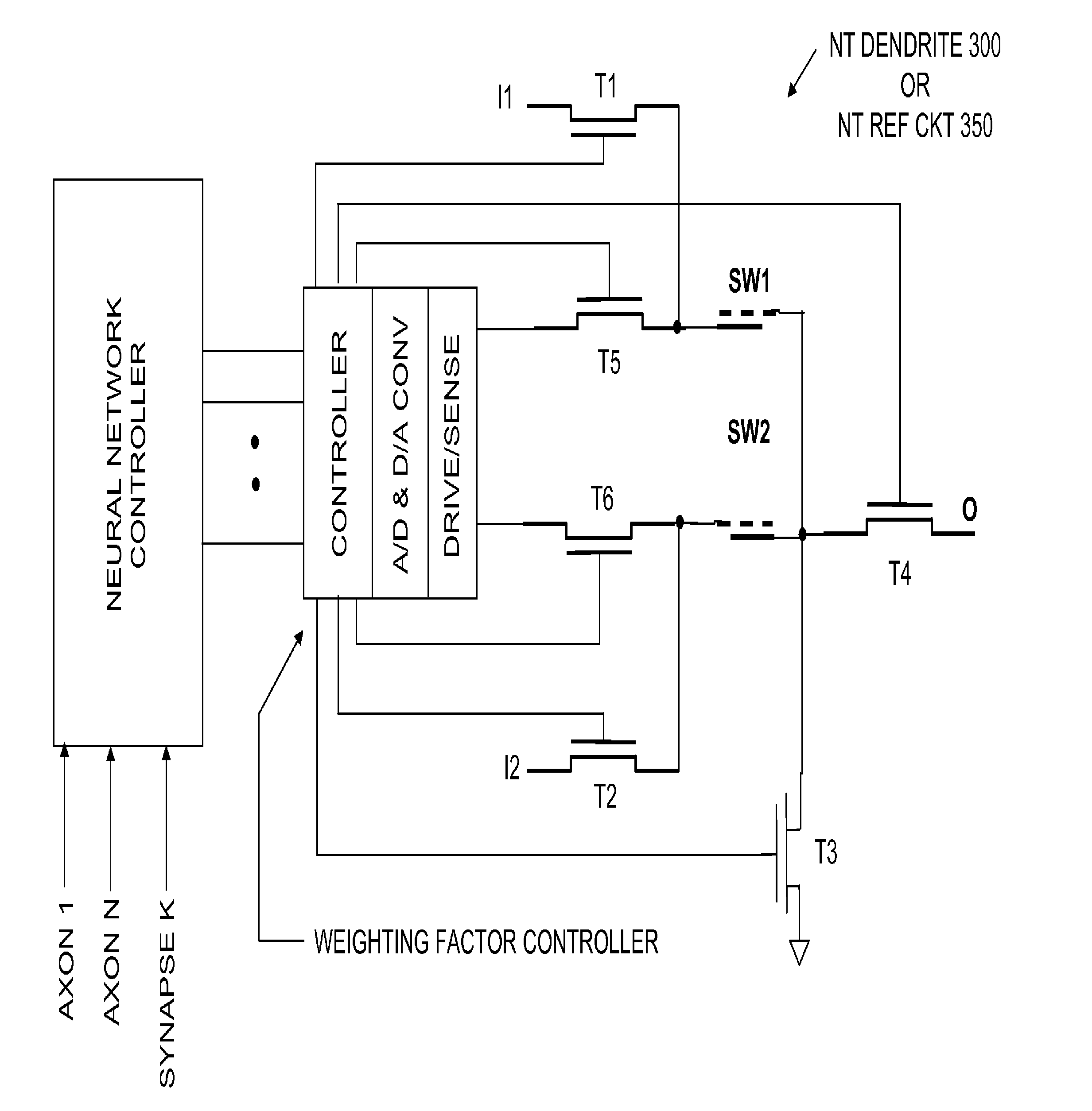
[0033]Nonvolatile nanotube switches enable new electronic implementations based on nanotube neural networks. One solution to the complexity and performance limitations of traditional electronic devices is the use of carbon nanotubes to fashion agile information processing circuits in analogy with biological neural networks. Nanotube-based circuit and network functions exhibit some of the desirable characteristics found in biological neural networks. For NT Neural Networks, these characteristics include:[0034]3D interconnections[0035]High device density[0036]Low power with nonvolatile nanotube switches[0037]Low noise because of relatively slow operation[0038]High fan-in compatibility via NT dendrite trees and high fan-out capability via NT axons[0039]Lowered cost, since there is no immediate need for very small technology nodes[0040]High reliability including tolerance to broad temperature ranges and high levels of radiation

[0041]Nanotube based circuits and networks using switches an...


PUM


Abstract

Physical neural networks based nanotechnology include dendrite circuits that comprise non-volatile nanotube switches. A first terminal of the non-volatile nanotube switches is able to receive an electrical signal and a second terminal of the non-volatile nanotube switches is coupled to a common node that sums any electrical signals at the first terminals of the nanotube switches. The neural networks further includes transfer circuits to propagate the electrical signal, synapse circuits, and axon circuits.

Description

CROSS REFERENCE TO RELATED APPLICATIONS[0001]This application is a U.S. national phase application under 35 U.S.C. §371 of International Patent Application No. PCT / US2009 / 038265 filed on Mar. 25, 2009, entitled CARBON NANOTUBE-BASED NEURAL NETWORKS AND METHODS OF MAKING AND USING SAME, which claims priority under 35 U.S.C. §119(e) to U.S. Provisional Patent Application No. 61 / 039,204, filed on Mar. 25, 2008, entitled CARBON NANOTUBE-BASED NEURAL NETWORKS AND METHODS OF MAKING AND USING SAME, the contents of each are incorporated herein in their entirety by reference.[0002]This application is related to the following applications, the entire contents of which are incorporated herein by reference in their entirety:[0003]U.S. patent application Ser. No. 11 / 280,786, filed 15 Nov. 2005, entitled TWO-TERMINAL NANOTUBE DEVICES AND SYSTEMS AND METHODS OF MAKING SAME;[0004]U.S. patent application Ser. No. 11 / 835,583, filed 8 Aug. 2006, entitled LATCH CIRCUITS AND OPERATION CIRCUITS HAVING SC...

Claims


Application Information

Patent Timeline
Patent Type & Authority Patents(United States)
IPC IPC(8): G11C11/54
CPCG06N3/063
Inventor BERTIN, CLAUDE L.SEGAL, BRENT M.BROCK, DARREN K.
Owner NANTERO
Learn More