Supercharge Your Innovation With Domain-Expert AI Agents!

Active array substrate and method for manufacturing the same

a technology of active array and substrate, which is applied in the direction of semiconductor devices, electrical apparatus, transistors, etc., can solve the problems of increasing production costs, and achieve the effects of excellent reliability, excellent performance and reliability, and cost-effectiveness

Active Publication Date: 2014-04-22
E INK HLDG INC
View PDF9 Cites 0 Cited by
  • Summary
  • Abstract
  • Description
  • Claims
  • Application Information

AI Technical Summary

Benefits of technology

This method significantly reduces production costs and enhances efficiency by minimizing photolithography steps while ensuring the reliability and performance of the active array substrate through the use of a protective layer that covers critical components, preventing cracking and erosion.

Problems solved by technology

However, each photolithography process implies an increase in production costs.

Method used


Image

  • Active array substrate and method for manufacturing the same
  • Active array substrate and method for manufacturing the same
  • Active array substrate and method for manufacturing the same

Examples


Embodiment Construction

[0014]Reference will now be made in detail to the present embodiments of the disclosure, examples of which are illustrated in the accompanying drawings. Wherever possible, the same reference numbers are used in the drawings and the description to refer to the same or like parts.

[0015]In the following detailed description, for purposes of explanation, numerous specific details are set forth in order to provide a thorough understanding of the disclosed embodiments. It will be apparent, however, that one or more embodiments may be practiced without these specific details. In other instances, well-known structures and devices are schematically shown in order to simplify the drawings.

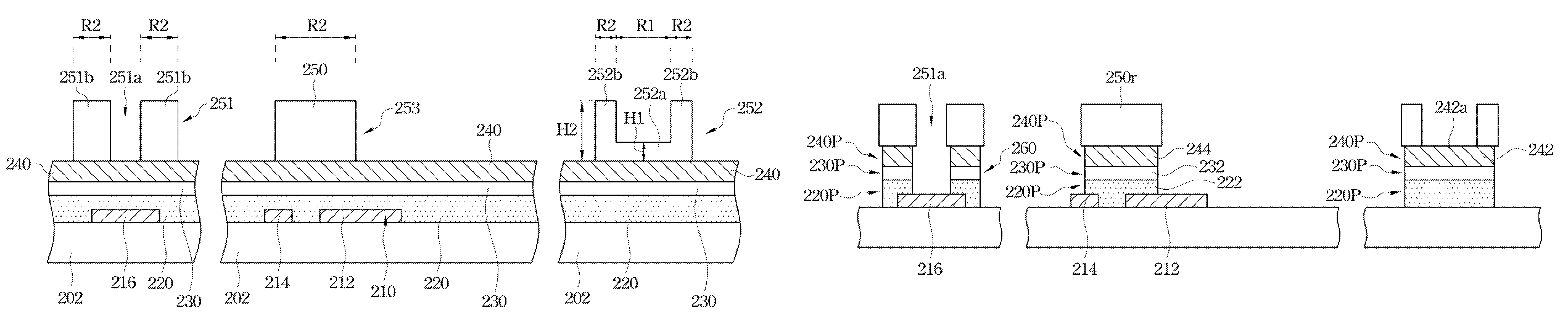
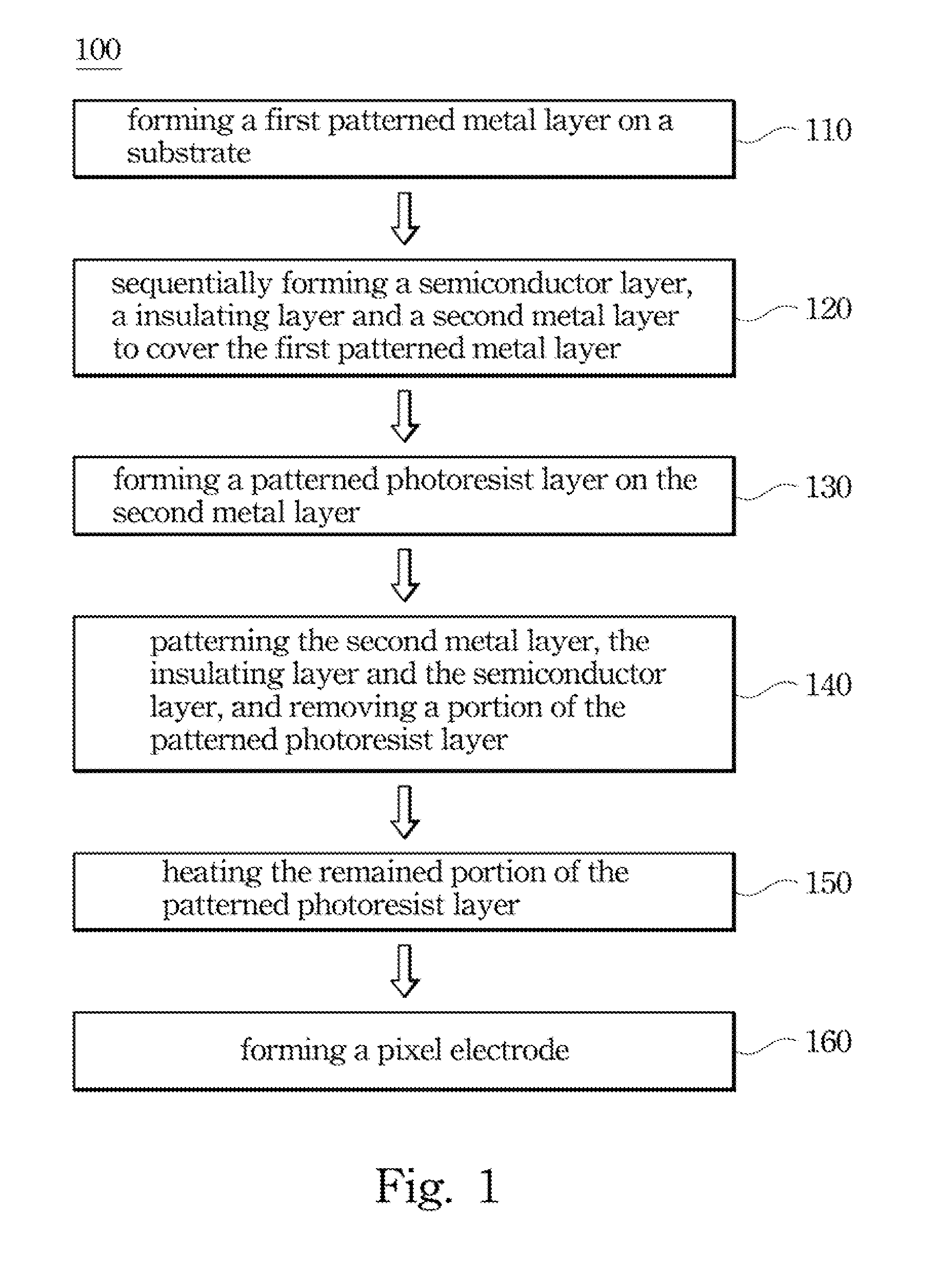
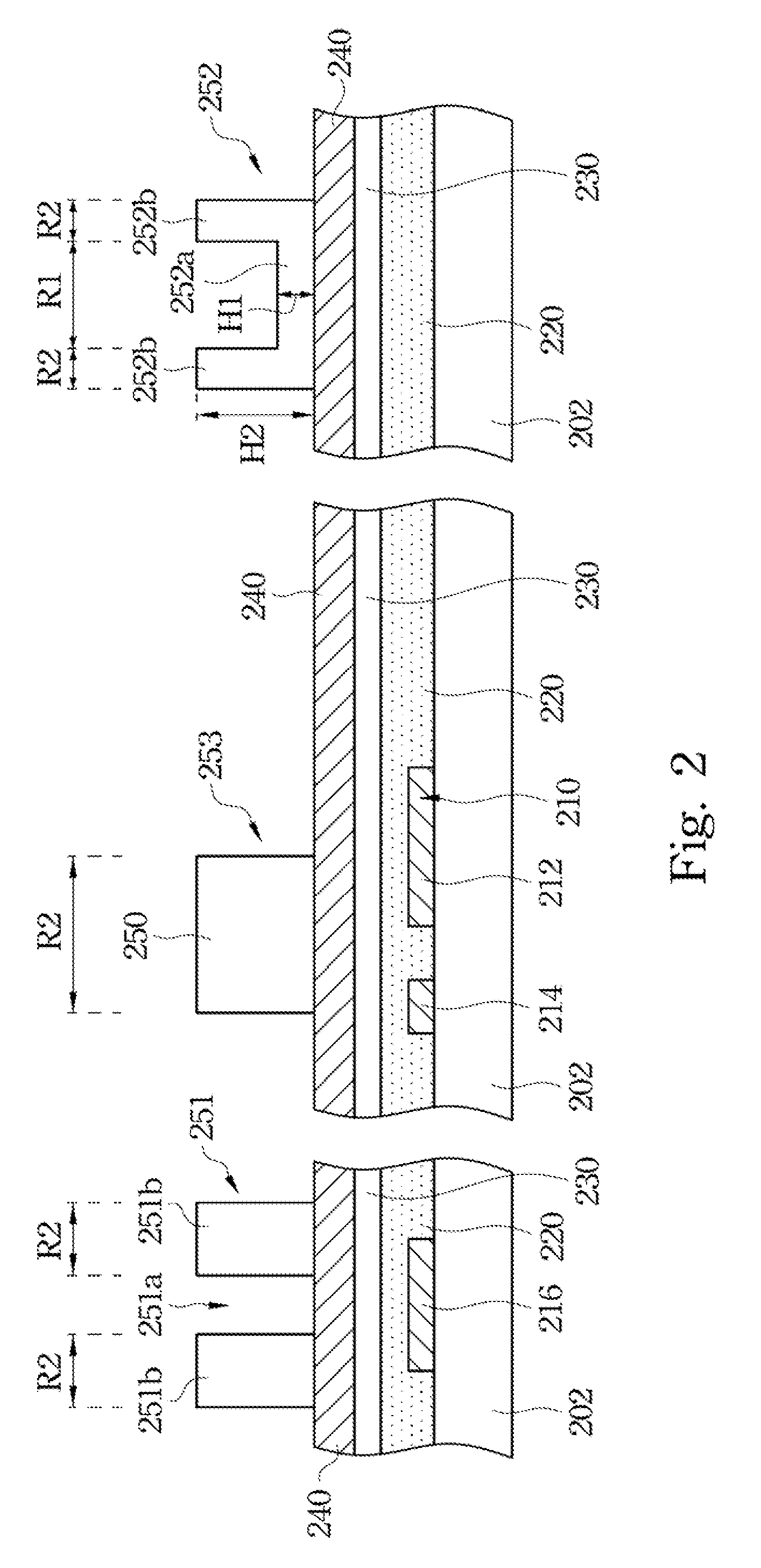
[0016]FIG. 1 is a flow chart showing a method 100 for manufacturing an active array substrate according to one embodiment of the present disclosure. FIGS. 2, 3A, 4 and 5 are cross-sectional views schematically illustrating the process steps of the method 100. The active array substrate fabricated by the meth...


PUM

PropertyMeasurementUnit
temperatureaaaaaaaaaa
thicknessaaaaaaaaaa

Abstract

Disclosed herein is a method for manufacturing an active array substrate. The method includes the steps of: forming a first patterned metal layer on a substrate; sequentially forming a semiconductor layer, an insulating layer and a second metal layer to cover the first patterned metal layer; forming a patterned photoresist layer on the second metal layer; patterning the second metal layer, the insulating layer and the semiconductor layer to form a second patterned metal layer, a patterned insulating layer and a patterned semiconductor layer, and removing a portion of the patterned photoresist layer; heating the remained portion of the patterned photoresist layer such that the remained portion is fluidized and transformed into a protective layer; and forming a pixel electrode.

Description

CROSS REFERENCE TO RELATED APPLICATIONS[0001]This application claims priority to U.S. Provisional Application Ser. No. 61 / 525,167 filed Aug. 18, 2011, and Taiwan Application Serial Number 101101600, filed Jan. 16, 2012, the disclosures of which are incorporated herein by reference in their entireties.BACKGROUND[0002]1. Technical Field[0003]The present disclosure relates to an active array substrate for a display device and a method for manufacturing the active array substrate.[0004]2. Description of Related Art[0005]Flat display devices such as liquid crystal display devices are widely applied in various types of electronic products. Flat display devices usually include active array substrates for driving the pixels of the display devices. In general, five photolithography processes are necessarily performed in conventional methods of fabricating the active array substrates. However, each photolithography process implies an increase in production costs. In recent years, a method usi...

Claims


Application Information

Patent Timeline
Patent Type & Authority Patents(United States)
IPC IPC(8): H01L29/786
CPCH01L27/1288
Inventor TANG, WEN-CHUNGSHU, FANG-ANTSAI, YAO-CHOUSHINN, TED-HONG
Owner E INK HLDG INC
Features
  • R&D
  • Intellectual Property
  • Life Sciences
  • Materials
  • Tech Scout
  • Unparalleled Data Quality
  • Higher Quality Content
  • 60% Fewer Hallucinations
Learn More