Check patentability & draft patents in minutes with Patsnap Eureka AI!

Doping apparatus for simultaneously injecting two dopants into a semiconductor melt at different positions and method for manufacturing silicon single crystal using the doping apparatus

a technology of semiconductor melt and doping apparatus, which is applied in the direction of crystal growth process, polycrystalline material growth, and under a protective fluid, can solve the problems of cumbersome operation and complicated, and achieve the effect of high monocrystallization and reducing the loss of shape in the ingo

Active Publication Date: 2014-05-06
SUMCO TECHXIV
View PDF19 Cites 0 Cited by
  • Summary
  • Abstract
  • Description
  • Claims
  • Application Information

AI Technical Summary

Benefits of technology

[0019]Accordingly, using one doping device, two types of dopants can be injected into the semiconductor melt substantially at the same time. Thus, dopant injecting operation for codoping can be considerably simplified.
[0021]Since the communicating hole is shaped in an elongated hole, the liquefied dopant is prevented from being accumulated due to surface tension or the like. Thus, the liquefied dopant can be quickly delivered into the semiconductor melt.
[0024]In this arrangement, since the second dopant accommodating portion has the conduit tube, the second dopant liquefied in the dopant holder of the second dopant accommodating portion can be injected into the semiconductor melt without scattering of the liquefied dopant. Especially, by soaking the conduit tube in the melt when the second dopant is liquefied and doped, scattering of the liquefied dopant can be reliably prevented.
[0026]In this arrangement, since the vent for degassing is provided on the cover portion of the doping device, pressure in an outer space and an inner space surrounded by the cover portion can be adjusted to prevent the liquefied Ge from being accumulated. Thus, the liquefied Ge can be quickly doped into the semiconductor melt from the communicating hole. In addition, the inner space of the cover portion that covers the Ge of the dopant holder is not hermetically sealed because of the vent. Thus, the semiconductor melt is not sucked into the doping device after being dropped off or thus the doping device is not cracked.
[0028]In this arrangement, when the upper end of the cover portion of the second dopant accommodating portion is opened and the second dopant accommodating portion is suspended by engagement between the engaging pieces and the projections, the space is provided between the bottom of the first dopant accommodating portion and the upper end surface of the second dopant accommodating portion. Accordingly, the inside and outside of the cover portion of the second dopant accommodating portion can be communicated. When the second dopant held by the dopant holder is liquefied, the liquefied dopant can be prevented from being accumulated around the communicating hole due to a pressure state within the cover portion. Thus, the liquefied dopant can be quickly diffused in the semiconductor melt through the conduit tube.
[0032]As compared with an arrangement for preparing a silicon melt by melting polycrystal silicon (semiconductor wafer material) and the second dopant together and then injecting into the silicon melt the first dopant evaporated after an elapse of a predetermined time, the arrangement according to the aspect of the invention can provide a more highly-monocrystallized ingot and can reduce loss of shape in the ingot.

Problems solved by technology

Thus, operation may be cumbersome and complicated.

Method used


Image

  • Doping apparatus for simultaneously injecting two dopants into a semiconductor melt at different positions and method for manufacturing silicon single crystal using the doping apparatus
  • Doping apparatus for simultaneously injecting two dopants into a semiconductor melt at different positions and method for manufacturing silicon single crystal using the doping apparatus
  • Doping apparatus for simultaneously injecting two dopants into a semiconductor melt at different positions and method for manufacturing silicon single crystal using the doping apparatus

Examples


Embodiment Construction

[0044]Exemplary embodiment(s) of the invention will be described below with reference to the attached drawings.

1. Overall Arrangement

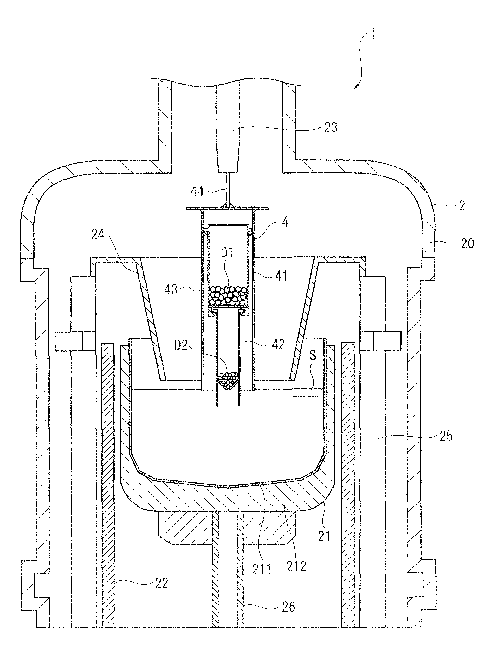
[0045]FIG. 1 shows an arrangement of a pulling-up device 1 according to an embodiment of the invention.

[0046]The pulling-up device 1 includes a pulling-up device body 2 and a doping device 4.

[0047]The pulling-up device body 2 includes a chamber 20, a crucible 21 disposed inside the chamber 20, a heater 22 for heating the crucible 21 by heat radiation, a pulling-up portion 23, a shield 24 and a heat insulating cylinder 25.

[0048]Inert gas such as argon gas is introduced into the chamber 20 from above to below. Pressure in the chamber 20 is controllable. When doping is performed, the pressure in the chamber 20 is 5332 Pa or more and 79980 Pa or less.

[0049]The crucible 21 is used to melt polycrystal silicon, from which a semiconductor wafer is made, to yield a silicon melt. The crucible 21 includes: a first crucible 211 made of quartz and shaped in a cylin...


PUM

PropertyMeasurementUnit
pressureaaaaaaaaaa
pressureaaaaaaaaaa
angleaaaaaaaaaa

Abstract

A doping device includes a first dopant accommodating portion including an opening on an upper portion to accommodate a first dopant that is evaporated near a surface of a semiconductor melt; a second dopant accommodating portion including a dopant holder that holds a second dopant that is liquefied near the surface of the semiconductor melt while including a communicating hole for delivering the liquefied dopant downwardly, and a conduit tube provided on a lower portion of the dopant holder for delivering the liquefied dopant flowed from the communicating hole to the surface of the semiconductor melt; and a guide provided by a cylinder body of which a lower end is opened and an upper end is closed for guiding dopant gas generated by evaporation of the first dopant to the surface of the semiconductor melt.

Description

[0001]This application is a U.S. National Phase Application under 35 USC 371 of International Application PCT / JP2008 / 059509 filed May 23, 2008.TECHNICAL FIELD[0002]The invention relates to a doping device and a method for manufacturing a silicon monocrystal.BACKGROUND ART[0003]For growing a monocrystal by a CZ (Czochralski) method, so-called codoping has been performed in which a primary dopant such as red phosphorus (P) or arsenic (As) that is solid at normal temperature and is evaporated near a surface of a semiconductor melt is injected together with a secondary dopant such as germanium that is solid at normal temperature and is liquefied near the surface of the semiconductor melt.[0004]For codoping, the secondary dopant is injected into the semiconductor melt and then dopant gas generated by evaporation of the primary dopant is squirted onto the semiconductor melt.[0005]However, when the secondary dopant is directly dropped into the semiconductor melt, the semiconductor melt sca...

Claims


Application Information

Patent Timeline
Patent Type & Authority Patents(United States)
IPC IPC(8): C30B15/04
CPCC30B29/06C30B11/04C30B30/00C30B15/04Y10T117/1032Y10T117/1056Y10T117/1024Y10T117/10Y10T117/1084
Inventor NARUSHIMA, YASUHITOKAWAZOE, SHINICHIOGAWA, FUKUOKUBOTA, TOSHIMICHI
Owner SUMCO TECHXIV
Features
  • R&D
  • Intellectual Property
  • Life Sciences
  • Materials
  • Tech Scout
  • Unparalleled Data Quality
  • Higher Quality Content
  • 60% Fewer Hallucinations
Learn More