Semiconductor device having lateral diode
a technology of lateral diodes and semiconductor devices, which is applied in the direction of diodes, semiconductor devices, electrical devices, etc., can solve the problems of avalanche breakdown and inability to improve avalanche capability, and achieve the effect of improving avalanche capability and reverse recovery capability
- Summary
- Abstract
- Description
- Claims
- Application Information
AI Technical Summary
Benefits of technology
Problems solved by technology
Method used
Image

Examples
first embodiment
[0046](First Embodiment)
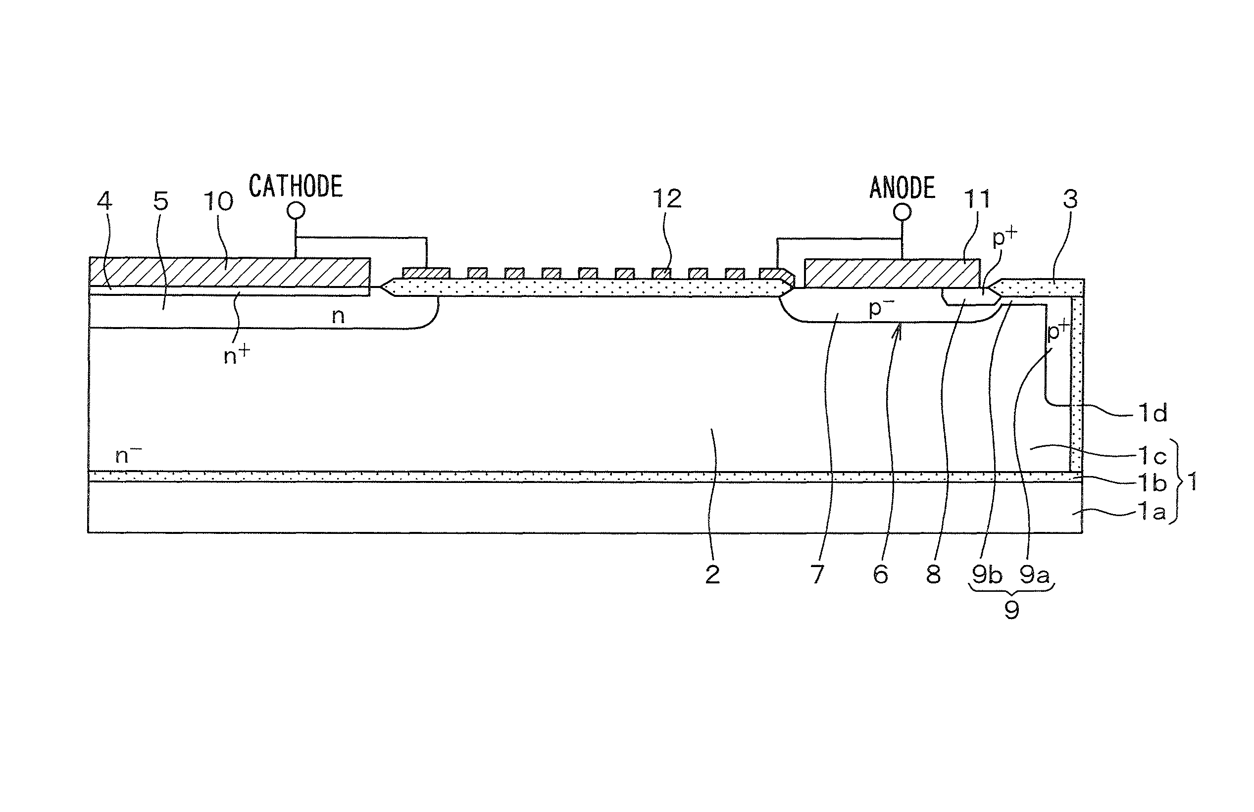
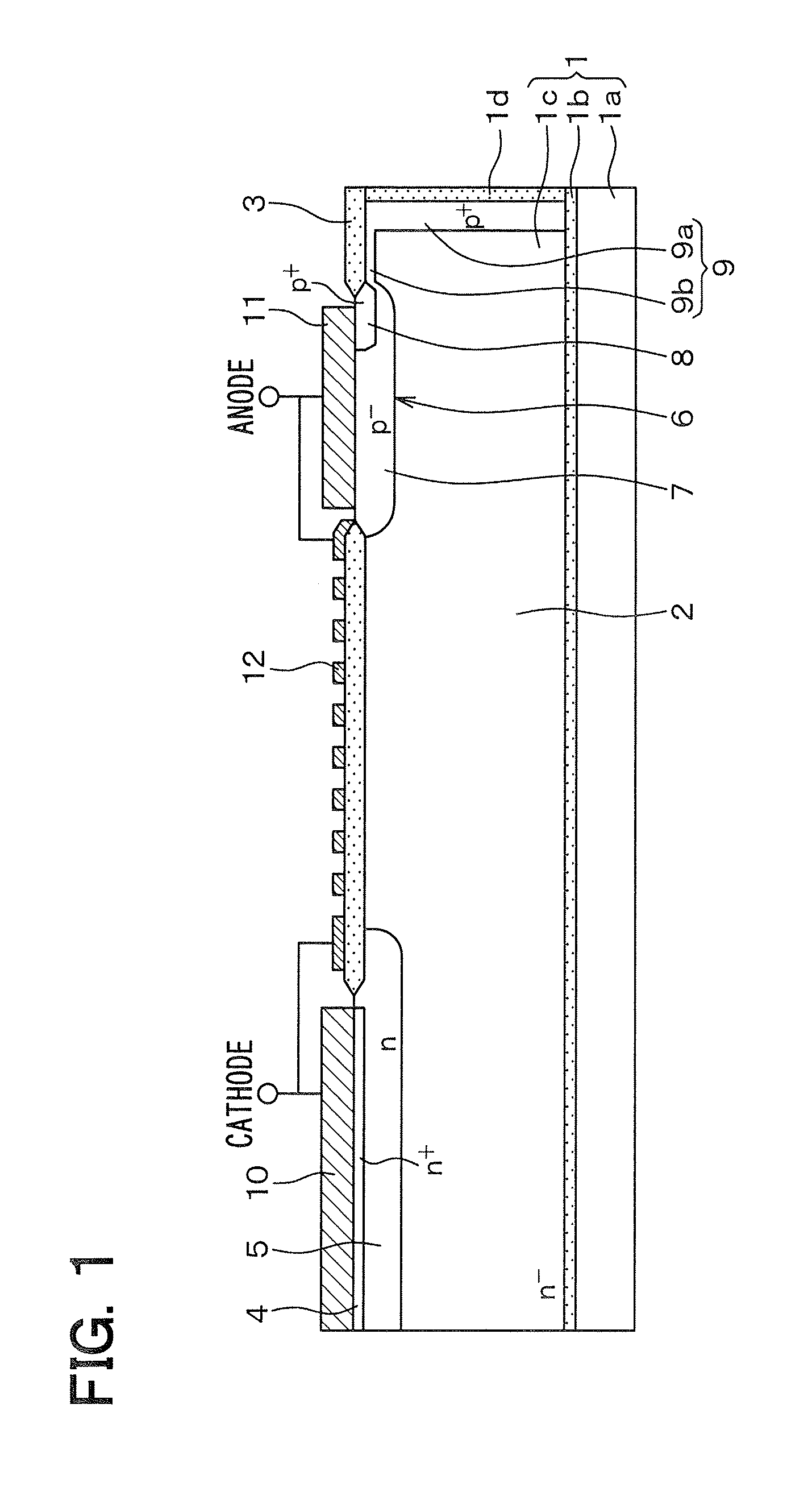
[0047]A semiconductor device having a lateral diode according to a first embodiment of the present invention is described below with reference to FIGS. 1, and 2A and 2B. FIG. 1 is a cross-sectional view of the semiconductor device taken along the line I-I in FIG. 2B. FIG. 2A is a top view of one cell of the lateral diode of the semiconductor device. FIG. 2B is an enlarged view taken within a region R in FIG. 2A.
[0048]According to the first embodiment, as shown in FIG. 1, the lateral diode is formed by using a semiconductor substrate 1 as a SOI substrate. The semiconductor substrate 1 includes a supporting substrate 1a, a buried oxide (BOX) layer 1b on the supporting substrate 1a, and an active layer 1c on the BOX layer 1b. For example, the supporting substrate 1a can be a silicon substrate, and the active layer 1c can be a silicon layer. According to the first embodiment, the active layer 1c serves as an n−-type cathode layer 2. Each part of the lateral diode...
second embodiment
[0081](Second Embodiment)
[0082]A second embodiment of the present invention is described below with reference to FIG. 9. A difference between the first and second embodiments is the structure of the anode extension portion 9.
[0083]FIG. 9 is a diagram illustrating a cross-sectional view of a semiconductor device having a lateral diode according the second embodiment. As shown in FIG. 9, according to the second embodiment, the thickness of the first portion 9a of the anode extension portion 9 is less than the active layer 1c. Specifically, the first portion 9a extends from the surface of the active layer 1c and is terminated inside the active layer 1c without reaching the BOX layer 1b. Thus, about an upper half of the side surface of the trench isolation structure 1d is covered with the first portion 9a, but about a lower half of the side surface of the trench isolation structure 1d is not covered with the first portion 9a. About the lower half of the trench isolation structure 1d is ...
third embodiment
[0086](Third Embodiment)
[0087]A third embodiment of the present invention is described below with reference to FIG. 10. A difference between the first and third embodiments is the structure of the anode extension portion 9.
[0088]FIG. 10 is a diagram illustrating a cross-sectional view of a semiconductor device having a lateral diode according the third embodiment. As shown in FIG. 10, according to the third embodiment, the thickness of the first portion 9a of the anode extension portion 9 is less than the active layer 1c. Specifically, like the second embodiment, the first portion 9a extends from the surface of the active layer 1c and is terminated inside the active layer 1c without reaching the BOX layer 1b.
[0089]Further, according to the third embodiment, the anode extension portion 9 has no second portion 9b. Therefore, the first portion 9a is separated from the anode region 6.
[0090]Even in such a structure as shown in FIG. 10, the depletion layer can extend from the anode exten...
PUM
 Abstract
Description
Claims
Application Information
 - R&D Engineer
- R&D Manager
- IP Professional
- Industry Leading Data Capabilities
- Powerful AI technology
- Patent DNA Extraction
Browse by: Latest US Patents, China's latest patents, Technical Efficacy Thesaurus, Application Domain, Technology Topic.
© 2024 PatSnap. All rights reserved.Legal|Privacy policy|Modern Slavery Act Transparency Statement|Sitemap