Multilinear image sensor with charge integration

a multi-linear, image sensor technology, applied in the field of linear tdi (time delay and integration) image sensors, can solve problems such as the inability to bring the surface regions

Inactive Publication Date: 2014-06-10
TELEDYNE E2V SEMICON SAS
View PDF10 Cites 6 Cited by
  • Summary
  • Abstract
  • Description
  • Claims
  • Application Information

AI Technical Summary

Problems solved by technology

It is therefore not possible to bring the surface regions to potentials different from one another.

Method used


Image

  • Multilinear image sensor with charge integration
  • Multilinear image sensor with charge integration
  • Multilinear image sensor with charge integration

Examples


Embodiment Construction

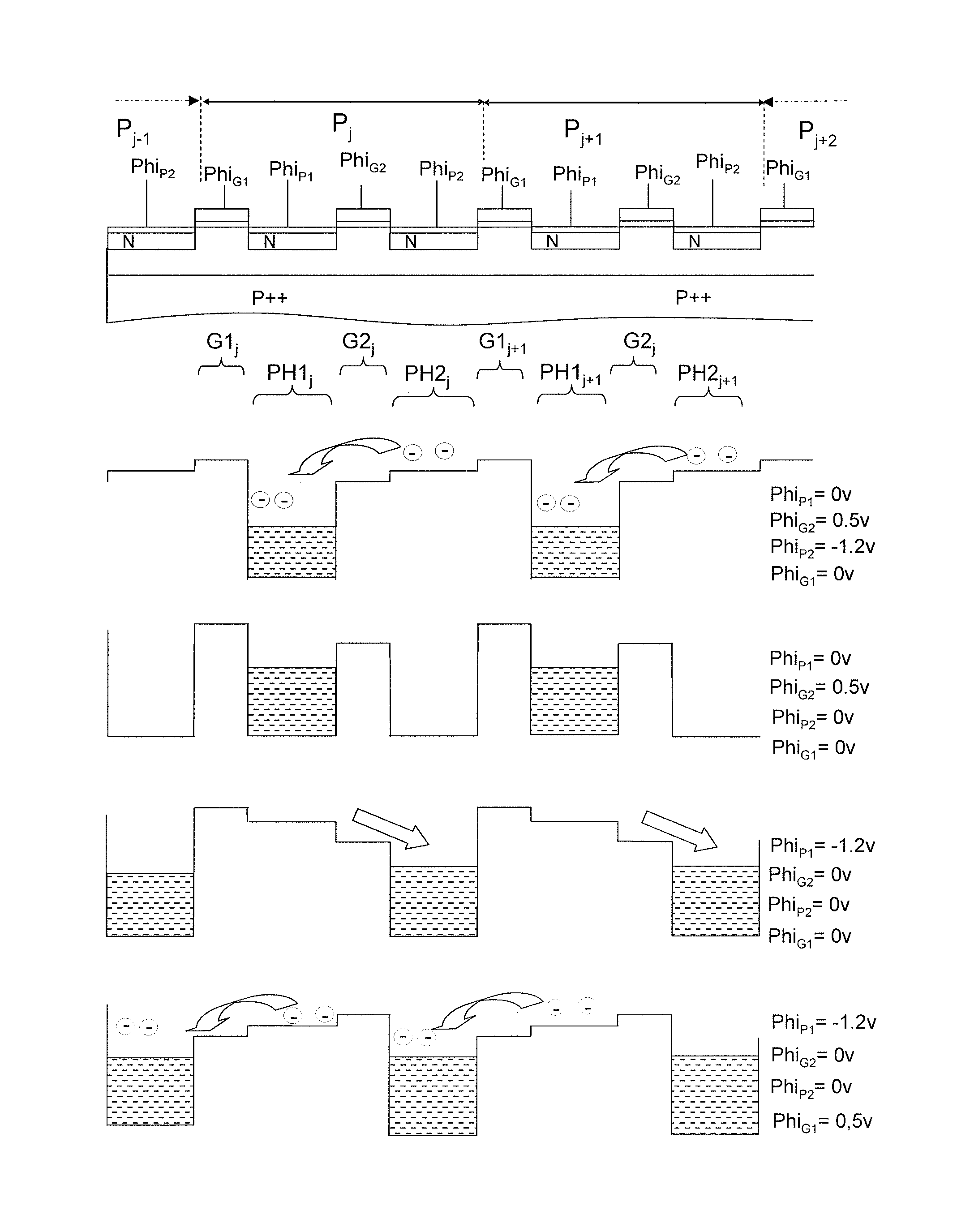
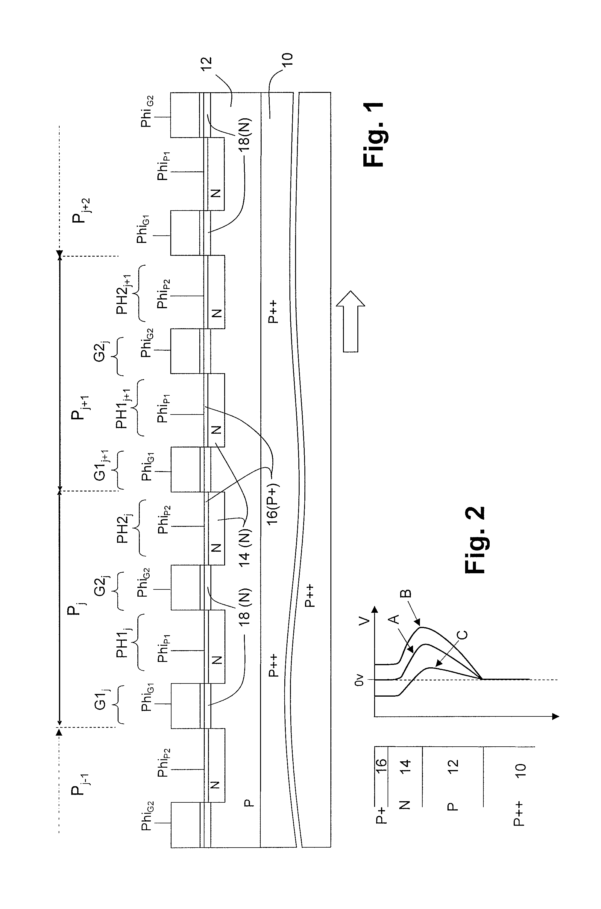
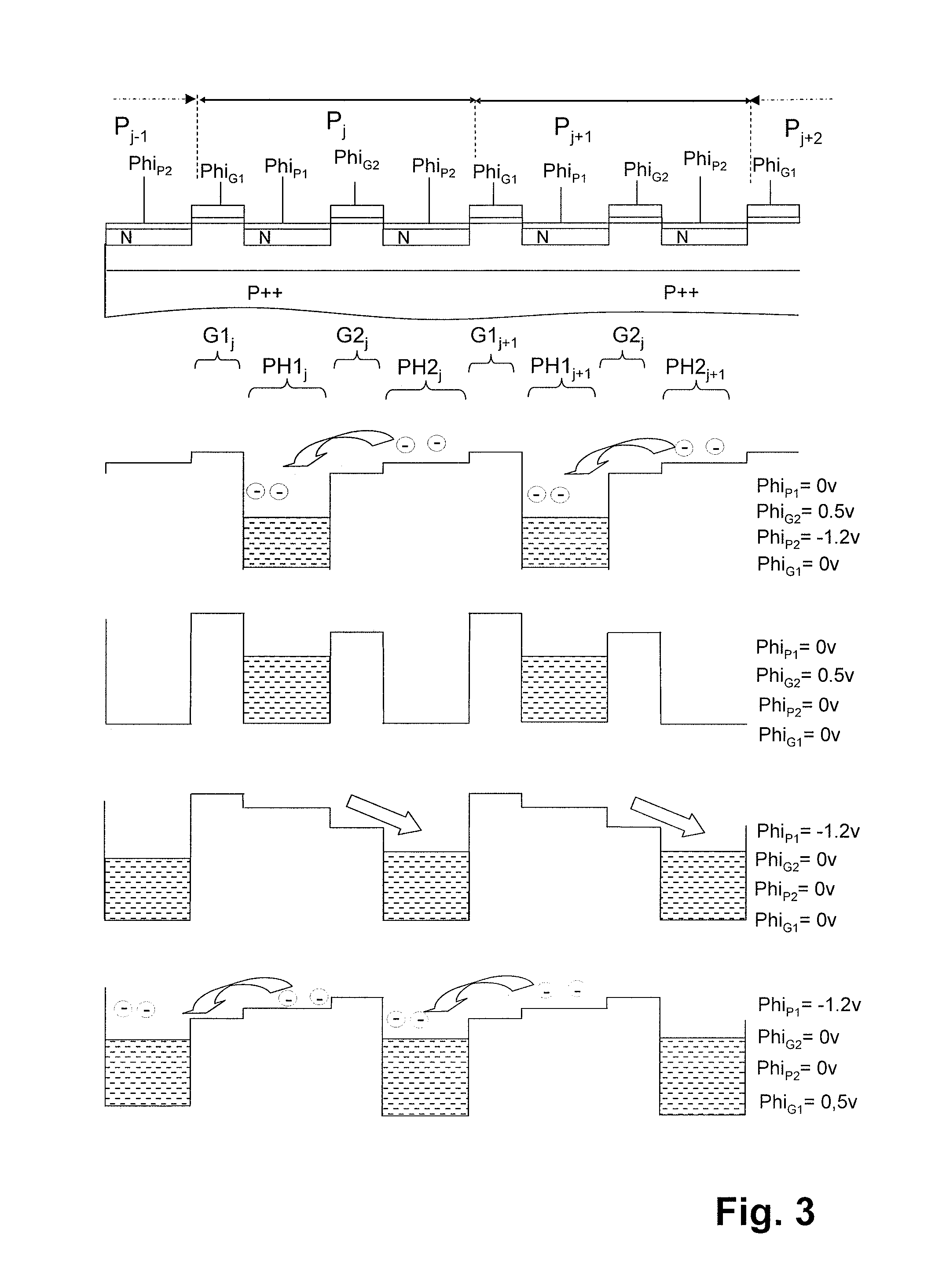
[0051]The cross-sectional view of FIG. 1 shows several successive pixels, of one and the same column, in a image sensor array comprising N adjacent rows each of P pixels, the array being intended to operate in TDI mode. Each row of rank j (j=1 to N) successively reads one and the same image row during a synchronized scan of the image relative to the array in the direction perpendicular to the direction of the rows. The charges of the pixels of the same rank i (i=1 to P) of the various rows correspond to the observation of one and the same image point and these charges are accumulated in order to obtain a larger signal (for a given exposure time of each row of pixels) than if only one row saw the image, improving the signal-to-noise ratio.

[0052]Essentially, the pixels Pj and Pj+1 of rank j and j+1 respectively one column have been shown.

[0053]The pixels are formed in a semiconductor substrate 10 the top part of which is an lightly doped epitaxial semiconductor layer 12. In this examp...


PUM


Abstract

The invention relates to linear time-delay and integration sensors (or TDI sensors). According to the invention, adjacent pixels of the same rank comprise, alternately, at least one photodiode and one transfer gate adjacent to the photodiode, the photodiodes comprising a common reference region of a first conductivity type, in which an individual region of opposite conductivity type is formed, itself covered by a individual surface region of the first conductivity type, characterized in that the surface regions of two photodiodes located on either side of a transfer gate are electrically separated so as to be able to be brought to different potentials in order to create potential wells and potential barriers allowing accumulation and transfer of charges as desired.

Description

CROSS-REFERENCE TO RELATED APPLICATIONS[0001]The present application is the U.S. National Stage of International Application No. PCT / EP2010 / 068694, filed on Dec. 2, 2010; which Application claims priority benefit of French Application No. 0958796, filed Dec. 9, 2009.TECHNICAL FIELD[0002]The invention relates to linear TDI (time-delay and integration) image sensors (or TDI sensors) in which an image of a row of points in an observed scene is reconstructed by adding successive images taken by several photosensitive rows by successively observing the same row of the scene as the scene scrolls before the sensor.BACKGROUND ART[0003]These sensors are used for example in scanners. They comprise a linear array of several parallel rows of photosensitive pixels. The sequencing of the control circuits of the various rows (control of the exposure time and then control of the readout of the photogenerated charges) is synchronized with respect to the relative scrolling between the scene and the s...

Claims


Application Information

Patent Timeline
Patent Type & Authority Patents(United States)
IPC IPC(8): H01L31/062
CPCH01L27/14812H01L27/14856H04N25/71
Inventor MAYER, FREDERIC
Owner TELEDYNE E2V SEMICON SAS
Why Eureka
Try Eureka