

Structure and method to measure waveguide power absorption by surface plasmon element
- Summary
- Abstract
- Description
- Claims
- Application Information
AI Technical Summary
Benefits of technology
Problems solved by technology
Method used
Image

Examples
Embodiment Construction
[0018]In the following detailed description, numerous specific details are set forth to provide a full understanding of the present invention. It will be apparent, however, to one ordinarily skilled in the art that the present invention may be practiced without some of these specific details. In other instances, well-known structures and techniques have not been shown in detail to avoid unnecessarily obscuring the present invention.
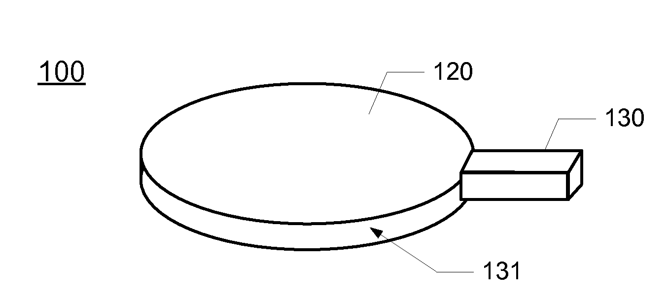
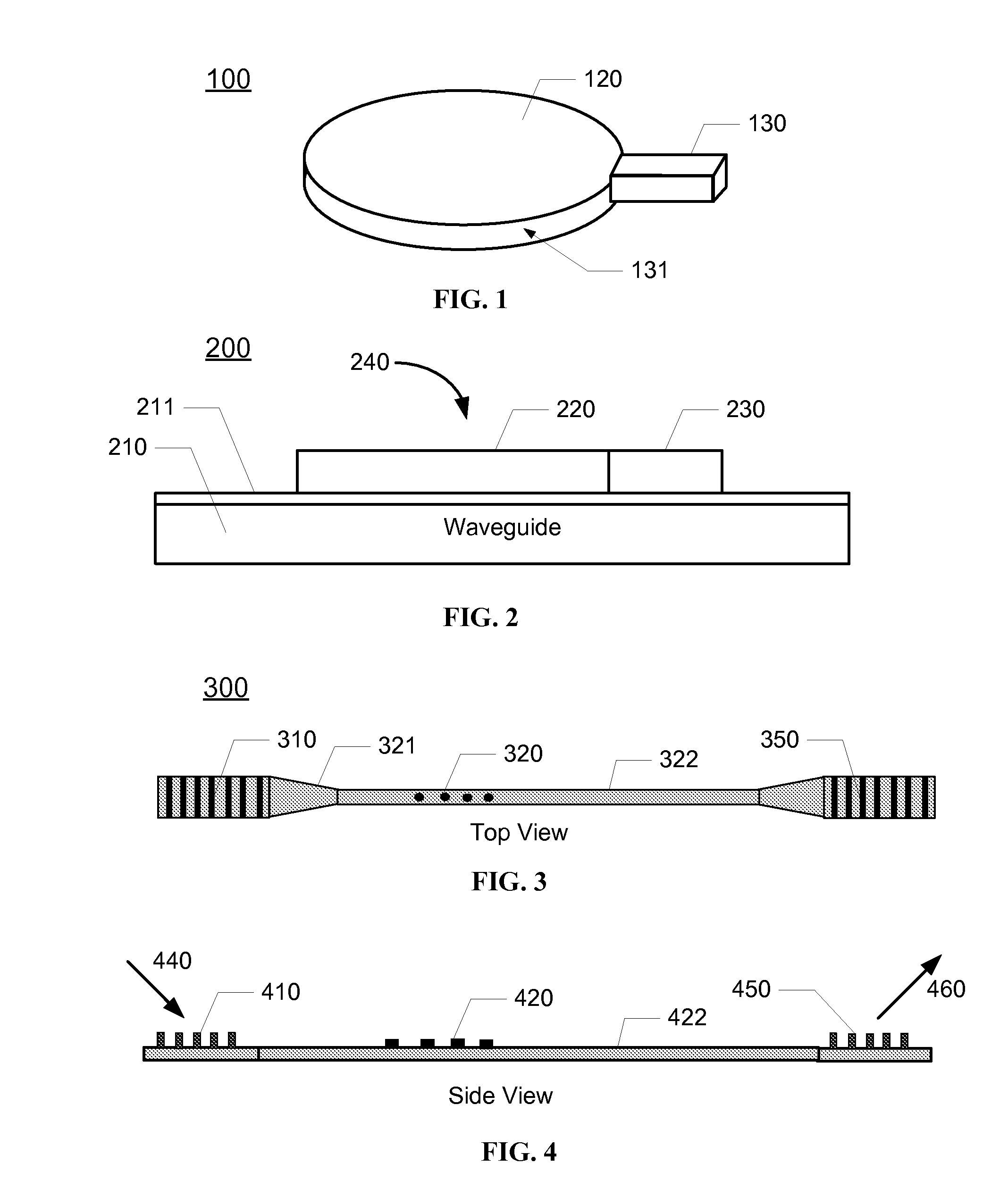
[0019]FIG. 1 is an illustration depicting a perspective view of a surface plasmon receptor disk type NFT 100 comprising a disk section 120 that has a side 131 and a pin section 130 connected to disk section 120.
[0020]FIG. 2 is a diagram depicting a cross-section view of an NFT arrangement 200 wherein a disk type NFT 240 comprises disk section 220 and pin section 230 coupled to a waveguide section 210. In one embodiment an optional intermediate layer 211 may be between the NFT 240 and waveguide section 210. In one embodiment, Intermediate layer 211 compris...
PUM
 Abstract
Description
Claims
Application Information