Apparatus and method for manufacturing compound semiconductor, and compound semiconductor manufactured thereby

a technology of compound semiconductor and manufacturing method, which is applied in the direction of semiconductor devices, coatings, chemical vapor deposition coatings, etc., can solve the problem of reducing the uniformity of compound semiconductor crystal growth, and achieve the effect of reducing the uniformity of crystal growth

Active Publication Date: 2014-06-17
TOYODA GOSEI CO LTD
View PDF37 Cites 6 Cited by
  • Summary
  • Abstract
  • Description
  • Claims
  • Application Information

AI Technical Summary

Benefits of technology

[0007]In such an apparatus for manufacturing a compound semiconductor, if the satellite disc does not contact with the sapphire substrate uniformly, a temperature difference due to a contact condition is generated on the surface of the sapphire substrate on which a crystal of the compound semiconductor is epitaxially grown. This causes a problem of reducing in uniformity of crystal growth of the compound semiconductor. An object of the present invention is to inhibit a change in temperature distribution of a substrate surface on which a crystal of a compound semiconductor is epitaxially grown, in manufacturing the compound semiconductor by use of the MOCVD method.

Problems solved by technology

This causes a problem of reducing in uniformity of crystal growth of the compound semiconductor.

Method used


Image

  • Apparatus and method for manufacturing compound semiconductor, and compound semiconductor manufactured thereby
  • Apparatus and method for manufacturing compound semiconductor, and compound semiconductor manufactured thereby
  • Apparatus and method for manufacturing compound semiconductor, and compound semiconductor manufactured thereby

Examples


second exemplary embodiment

(Second Exemplary Embodiment of Support Member)

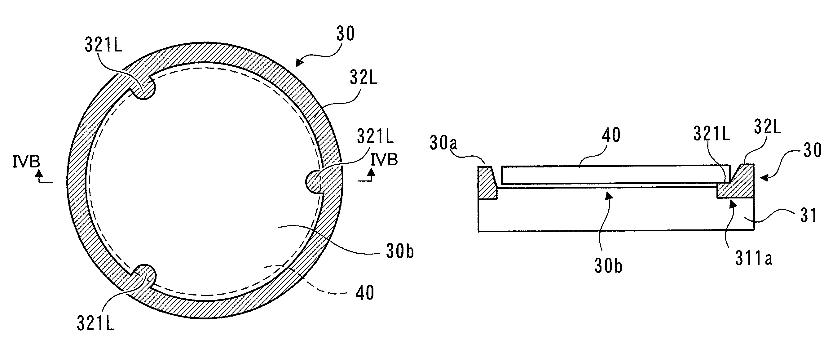
[0050]FIGS. 4A to 4C are views for illustrating a configuration of the substrate holders 30 of the second exemplary embodiment used in the above-described MOCVD apparatus 1. FIG. 4A is a top view of the substrate holder 30 on which a support member 32L having a ring shape is mounted. FIG. 4B is a cross-sectional view of FIG. 4A taken along a line IVB-IVB, in a case where the compound semiconductor substrate 40 is placed thereon. FIG. 4C is an enlarged cross-sectional view of a part at which the support member 32L of FIG. 4B is mounted. The same reference numerals are used for the same components as those in FIGS. 3A to 3C, and the description thereof is omitted. In FIG. 4A, the compound semiconductor substrate 40 (see FIG. 2) placed on the substrate holder 30 is shown with a broken line.

[0051]As shown in FIG. 4A, the ring-shaped support member 32L is mounted on the circumferential edge of the concave portion 30b of the substrate holder ...


PUM

PropertyMeasurementUnit
coefficient of thermal conductivityaaaaaaaaaa
distanceaaaaaaaaaa
widthaaaaaaaaaa

Abstract

Provided is an apparatus for manufacturing a compound semiconductor by use of metal organic chemical vapor deposition including: a reaction container; a holder on which a formed body is to be placed so that a formed surface of the formed body on which layers of a compound semiconductor are to be formed faces upward, the holder being arranged in the reaction container; and a material supply port supplying a material gas of the compound semiconductor into the reaction container from outside, wherein the holder includes a support member supporting the formed body so that an undersurface of the formed body and a top surface of the holder on which the formed body is to be placed keep a predetermined distance.

Description

BACKGROUND[0001]1. Technical Field[0002]The present invention relates to an apparatus and a method for manufacturing a compound semiconductor, and a compound semiconductor manufactured thereby.[0003]2. Related Art[0004]Conventionally, metal organic chemical vapor deposition (hereinafter, referred to as MOCVD method) is known as one of methods to grow a compound semiconductor crystal.[0005]As an apparatus for manufacturing a compound semiconductor by use of the MOCVD method, Japanese Patent Application Laid-Open Publication No. 2004-103708 describes an apparatus in which plural substrates being growth targets of compound semiconductor crystals are mounted on a holder formed of SiC inside of a reaction tube supplied with a material gas so that each of growth surfaces of the crystals faces upward, and then the holder is rotated to grow the crystals while the substrates are rotated.[0006]In an apparatus for manufacturing a compound semiconductor by use of the MOCVD method, a sapphire su...

Claims


Application Information

Patent Timeline
Patent Type & Authority Patents(United States)
IPC IPC(8): C23C16/458B05C13/02
CPCH01L21/02579H01L21/02576C23C16/4585H01L21/68771H01L21/0254C23C16/4584H01L21/68764H01L21/0262H01L21/68735C23C16/303C23C16/4583
Inventor YASUHARA, HIDEKIBANDOH, AKIRA
Owner TOYODA GOSEI CO LTD
Why Eureka
Try Eureka