

Ta sputtering target and method for producing the same
a sputtering target and sputtering technology, applied in the direction of sputtering coating, vacuum evaporation coating, coating, etc., can solve the problems of insufficient methods, insufficient uniform crystalline microstructure of the billet (slab), and insufficient ta sputtering target, so as to improve the uniform crystalline microstructure of the billet without lowering the yield
- Summary
- Abstract
- Description
- Claims
- Application Information
AI Technical Summary
Benefits of technology
Problems solved by technology
Method used
Image

Examples
example 1
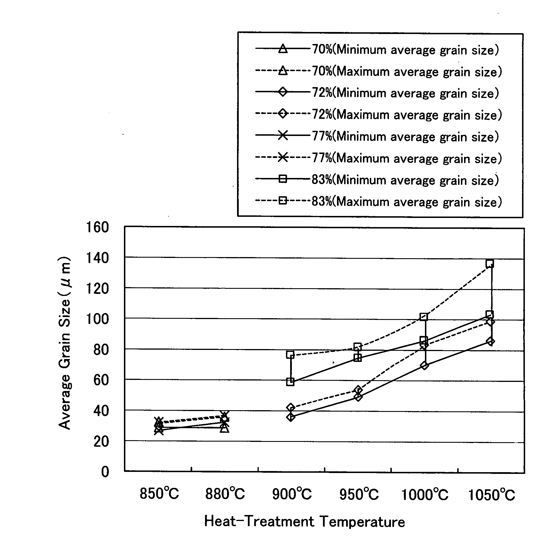
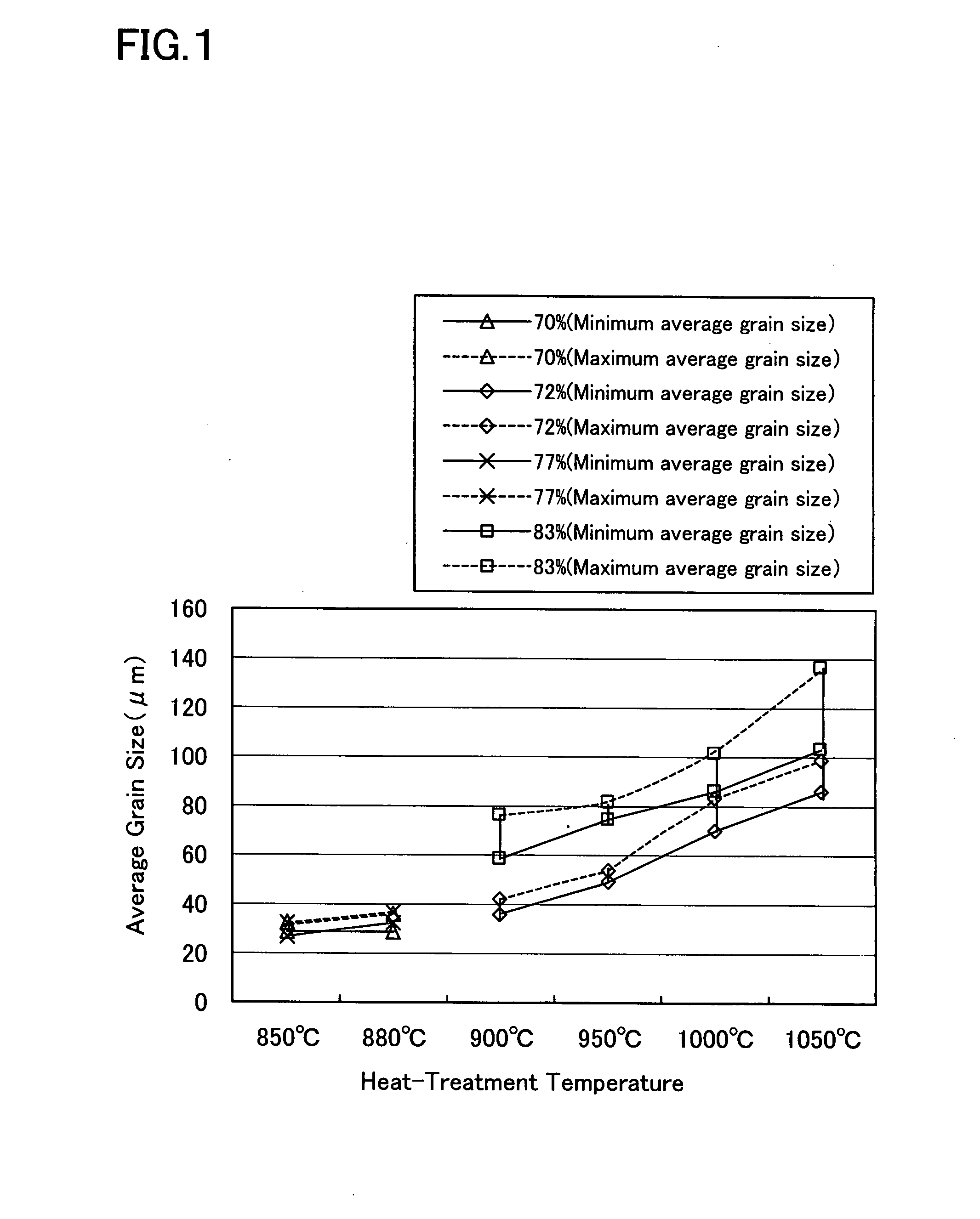
[0036]First, a Ta ingot having a size of 140 mmφ×200 mmL was subjected to stamp-forging and upset-forging operations alternatively repeated 3 times to thus obtain a primary forged billet, and then the latter was subjected to vacuum heat treatment (not more than 1.3×10⁻² Pa; 1050° C.). The resulting primary forged billet was then subjected to the same procedures used in the primary forging step to thus prepare a secondary forged billet. Then the secondary forged billet was subjected to the same vacuum heat treatment used above and thereafter, it was further subjected to a third forging step according to the same procedures used above. The surface of the resulting tertiary forged billet was processed (working with a lathe) to thus remove any defect such as surface defects, cracks and / or fogging or protective covering, then subjected to a cold rolling operation in 4 axial directions at a total draft percentage of 70%. The resulting rolled plate was subjected to a vacuum heat treatment ...
example 2
[0037]The surface-processed tertiary forged billet prepared according to the method described in Example 1 was subjected to a cold rolling operation in 6 axial directions at a total draft percentage of 70%. The resulting rolled plate was subjected to a vacuum heat treatment at 880° C. As a result, it was found that the average grain size on the whole surface of the resulting sputtering target fell within the range from 29 to 36 μm and that the standard deviation of the grain size thereof was found to be 17 μm.
example 3
[0038]The surface-processed tertiary forged billet prepared according to the method described in Example 1 was subjected to a cold rolling operation in 8 axial directions at a total draft percentage of 72% and the resulting rolled plate was subjected to a vacuum heat treatment at 900° C. As a result, it was found that the average grain size on the whole surface of the resulting sputtering target fell within the range from 36 to 42 μm and that the standard deviation of the grain size thereof was found to be 19 μm.
PUM
| Property | Measurement | Unit |
|---|---|---|
| aspect ratio | aaaaa | aaaaa |
| temperature | aaaaa | aaaaa |
| grain size | aaaaa | aaaaa |
Abstract
Description
Claims
Application Information