Electronic component mounting structure

a technology for mounting structures and components, applied in the direction of final product manufacturing, sustainable manufacturing/processing, semiconductor/solid-state device details, etc., can solve the problems of reducing the bonding area to be difficult to obtain sufficient reinforcement effect, deteriorating the repairability, etc., to achieve easy removal of cured resins, excellent repairability, and reusability of substrates

Active Publication Date: 2014-06-24
PANASONIC CORP
View PDF39 Cites 0 Cited by
  • Summary
  • Abstract
  • Description
  • Claims
  • Application Information

AI Technical Summary

Benefits of technology

[0008]In this connection, the invention intends to provide an electronic component mounting structure that can combine the repairability and the impact resistance.
[0014]According to the invention, an electronic component mounting structure that is excellent in the repairability such as the easy removability of the cured resin and the reusability of the substrate, allows the elongation of the resin per se to the impact at the time of drop to be able to play a role of bonding reinforcement without breaking and is excellent as well in the impact resistance can be realized.

Problems solved by technology

However, since these characteristics are in the trade-off relationship, when the impact resistance is considered most important and a resin is filled in an entire region of a gap between the BGA or CSP and the substrate to reinforce the bonding, a bonding area is increased to deteriorate the repairability.
By contrast, when the repairability is considered most important and portions where the resin is filled are restricted to four corners of the BGA or CSP, a bonding area is reduced to be difficult to obtain sufficient reinforcement effect.

Method used


Image

  • Electronic component mounting structure
  • Electronic component mounting structure
  • Electronic component mounting structure

Examples


Embodiment Construction

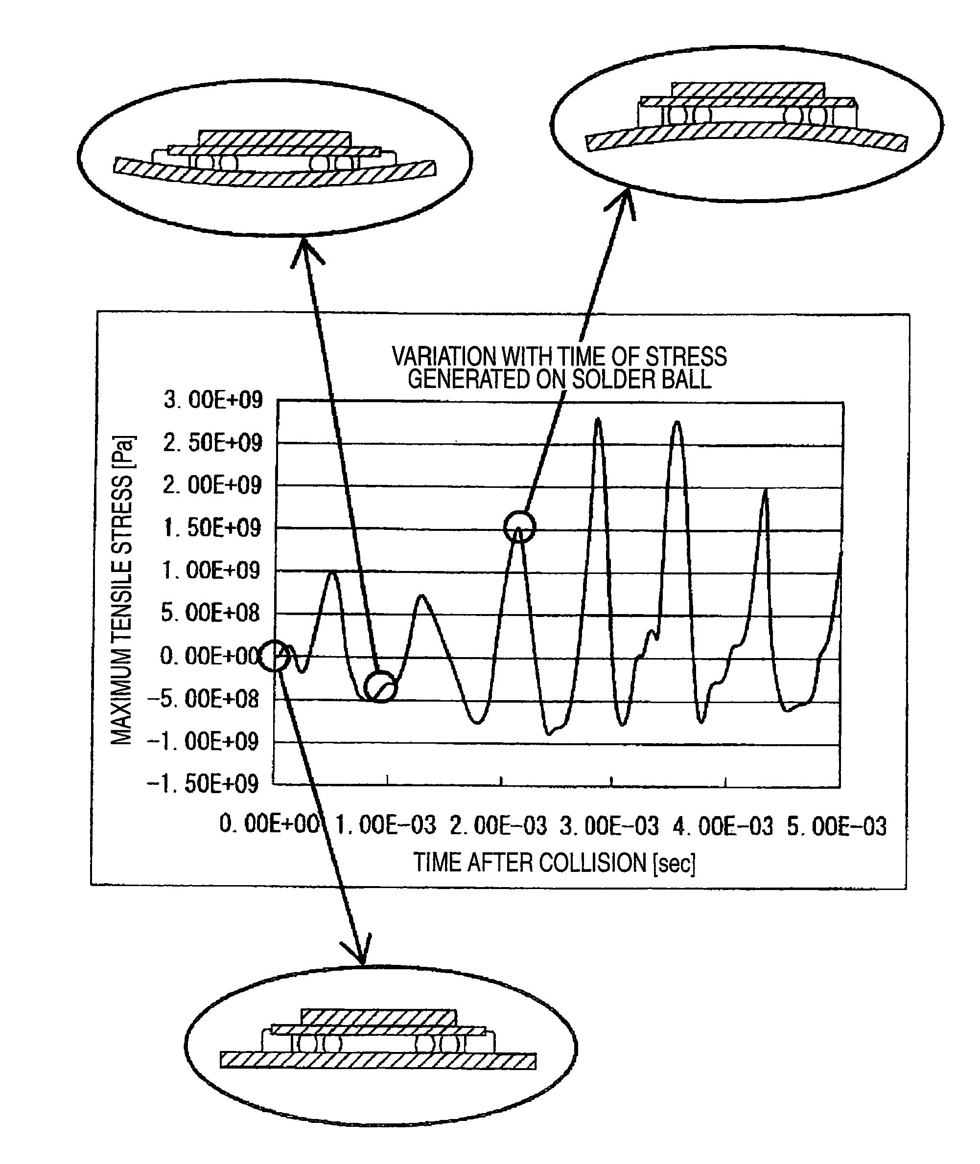
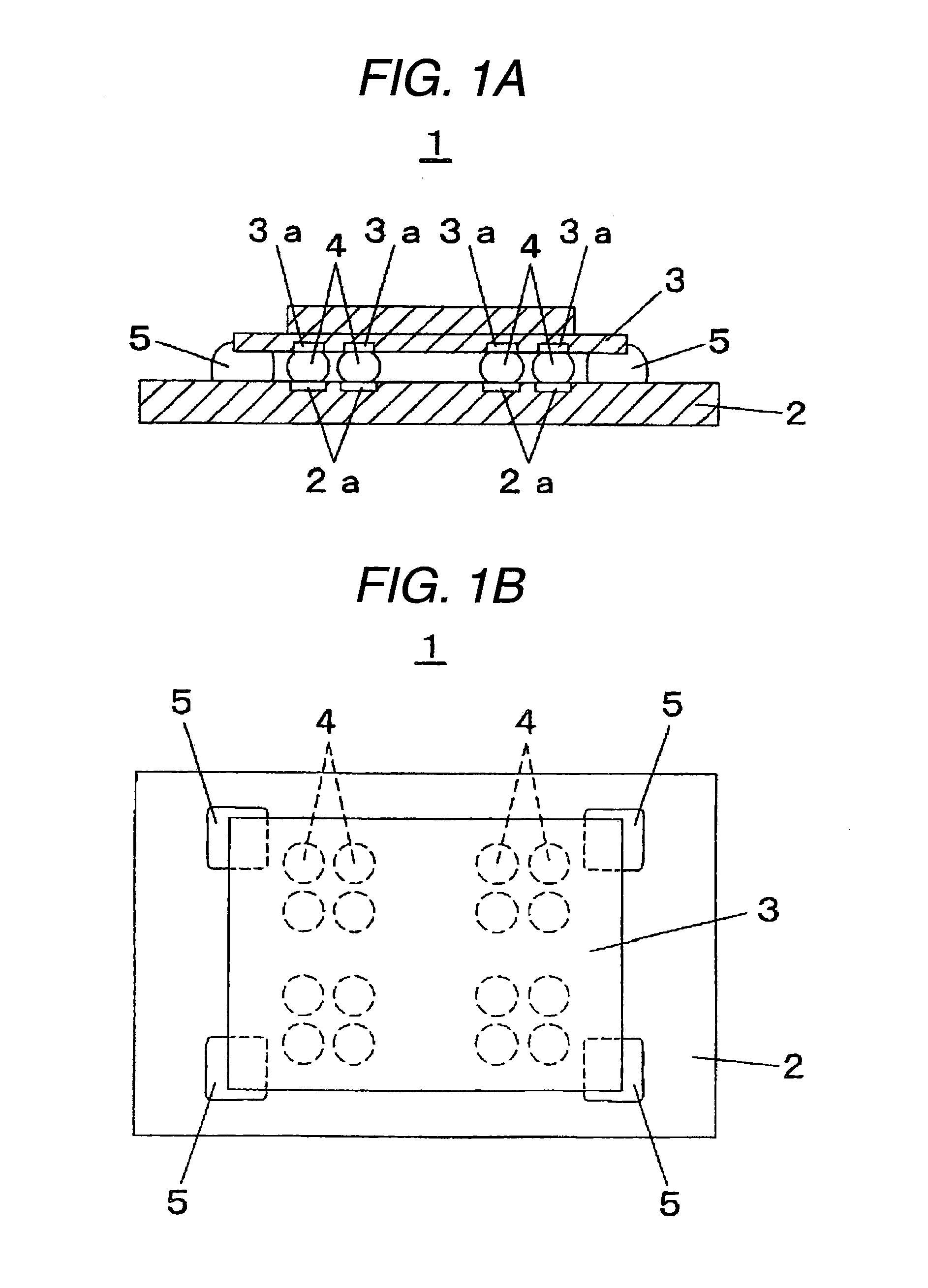
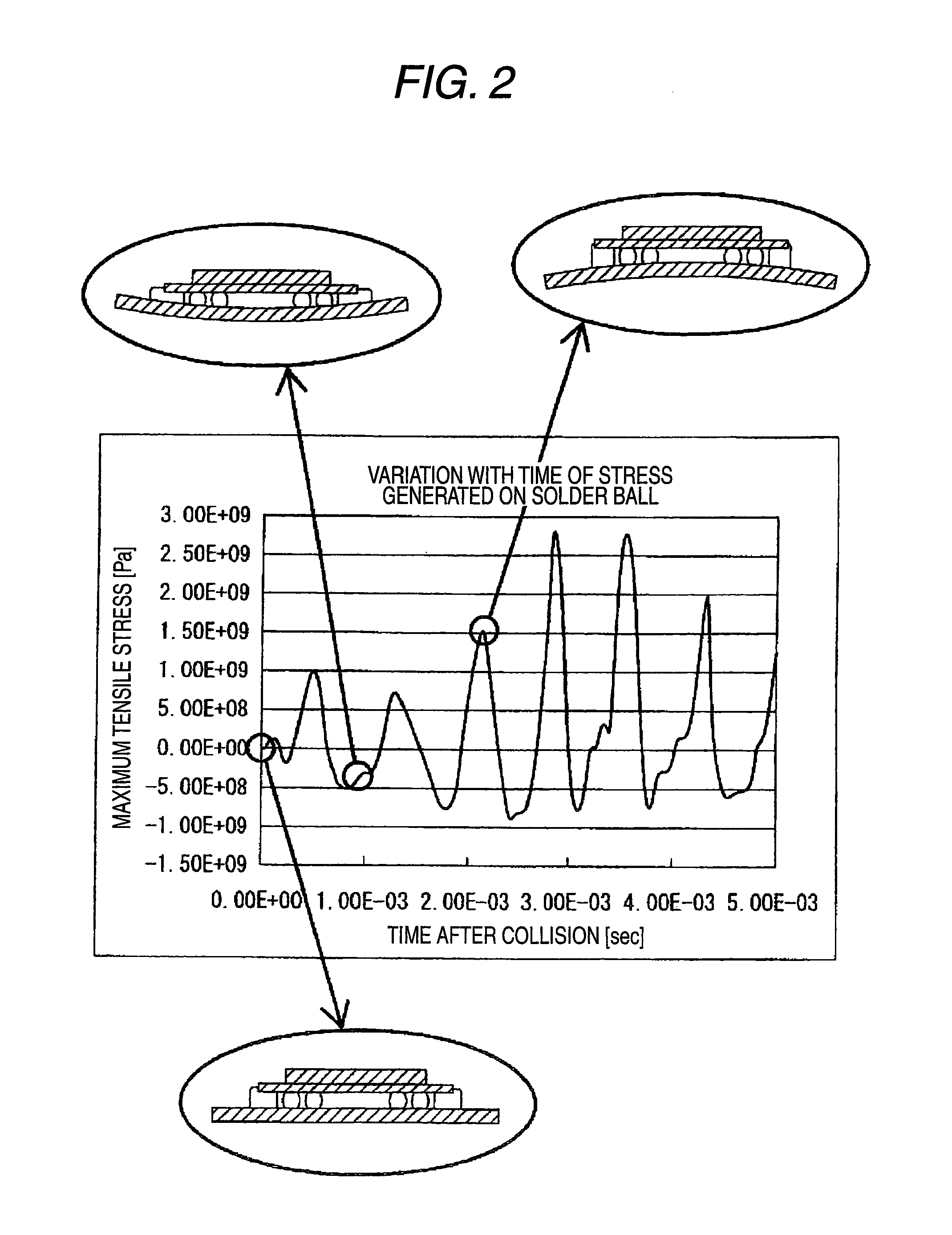
[0018]An embodiment of the invention will be described with reference to the drawings. FIG. 1A is a side view of an electronic component mounting structure of an embodiment of the invention and FIG. 1B is a plan view thereof. FIG. 2 is a diagram showing results obtained by analyzing, according to the finite element method, stresses generated on solder balls when an electronic component mounting structure of the embodiment of the invention is naturally fallen in a horizontal state.

[0019]In the beginning, an electronic component mounting structure of the embodiment will be described with reference to FIGS. 1A and 1B. In the drawing, an electronic component mounting structure 1 has a structure where a plurality of solder balls 4 disposed in plane between a substrate 2 and an electronic component 3 is melted to bond the electronic component 3 and the substrate 2 and a bond reinforcing resin 5 is filled between the electronic component 3 and the substrate 2 and cured. The solder balls 4 ...


PUM

PropertyMeasurementUnit
tensile elongationaaaaaaaaaa
thixotropic ratioaaaaaaaaaa

Abstract

The invention intends to provide an electronic component mounting structure where the repairability and the impact resistance are combined. In an electronic component mounting structure, a plurality of solder balls disposed in plane between an electronic component and a substrate is melted to bond the electronic component and the substrate and a resin of which tensile elongation after the curing is in the range of 5 to 40% is filled in portions that are gaps between the electronic component and the substrate and correspond to at least four corners of the electronic component to reinforce. Since the reinforcement area is small, the repairability such as the easy removability of the resin and the reusability of the substrate are excellent, the resin itself is allowed to expand to the impact at the drop to play a role of reinforcing the bonding without breaking, and the impact resistance is excellent as well.

Description

TECHNICAL FIELD[0001]The present invention relates to an electronic component mounting structure that is mounted on an electronic device such as a portable mobile.BACKGROUND ART[0002]As higher performance and more miniaturization of portable mobiles such as portable telephones and PDAs are forwarded, electronic components mounted thereon are demanded to be more densely mounted. As the results, in place of QFPs (Quad Flat Packages) of which substrate occupying area is large, flip-chip type packages such as BGA (Ball Grid Array) and CSP (Chip Size Package) are becoming a main stream in the packaging. In the BGA and CSP, different from the QFP where bonding terminals are laterally disposed, a plurality of solder balls (also called as solder bumps) is disposed on a bonding surface of a package, and the solder balls, after mounting on bonding terminals on the substrate side, are melted to establish electrical connection and physical bonding. Furthermore, when the stress due to the heat c...

Claims


Application Information

Patent Timeline
Patent Type & Authority Patents(United States)
IPC IPC(8): H05K1/16
CPCH05K3/3436H01L2224/73203H01L21/563Y10T428/23971H05K2203/0545H05K2201/0133H01L2924/3511H01L2924/15311Y10T428/31525H05K2201/10734H05K3/305H01L23/293Y02P70/50H01L23/29H01L23/31H05K1/18
Inventor YOSHINAGA, SEIICHIWADA, YOSHIYUKISAKAI, TADAHIKO
Owner PANASONIC CORP
Why Eureka
Try Eureka