Over-current detecting apparatus for switching element
a switching element and over-current detection technology, applied in the direction of electronic switching, pulse technique, instruments, etc., can solve the problems of increasing the overall cost of the over-current detection apparatus, requiring additional, and occupying space, so as to achieve the effect of occupying spa
- Summary
- Abstract
- Description
- Claims
- Application Information
AI Technical Summary
Benefits of technology
Problems solved by technology
Method used
Image
Examples
second embodiment
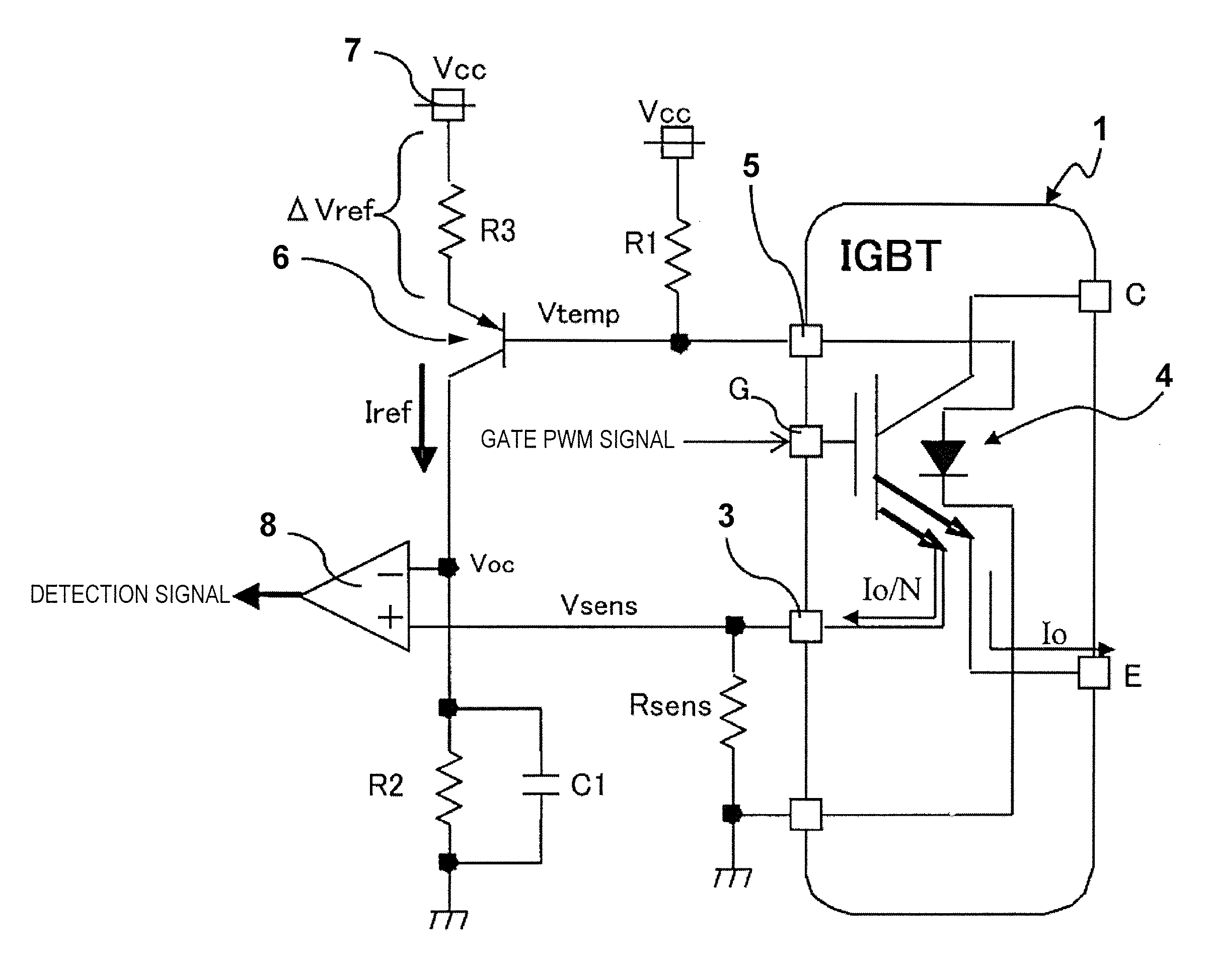
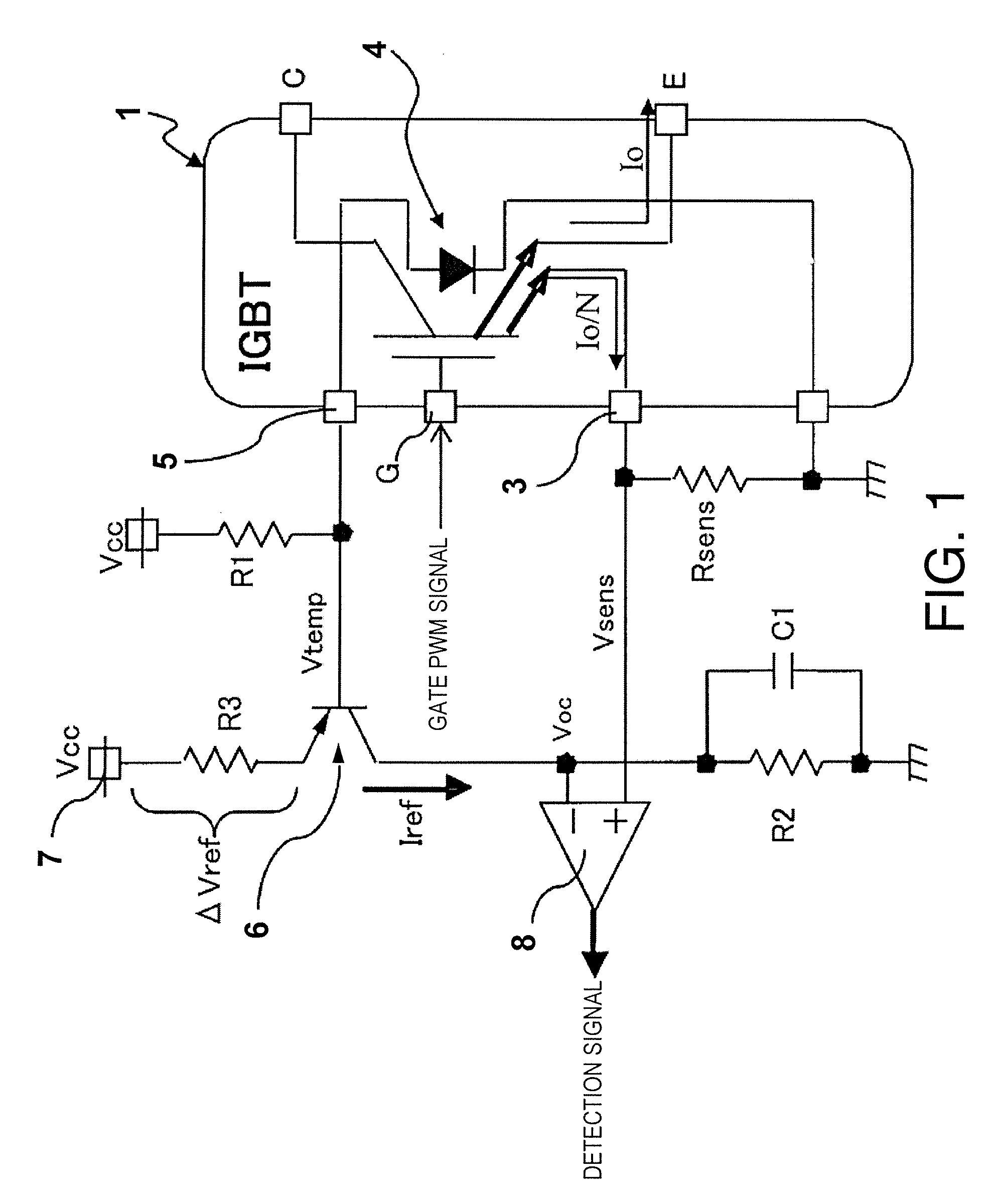
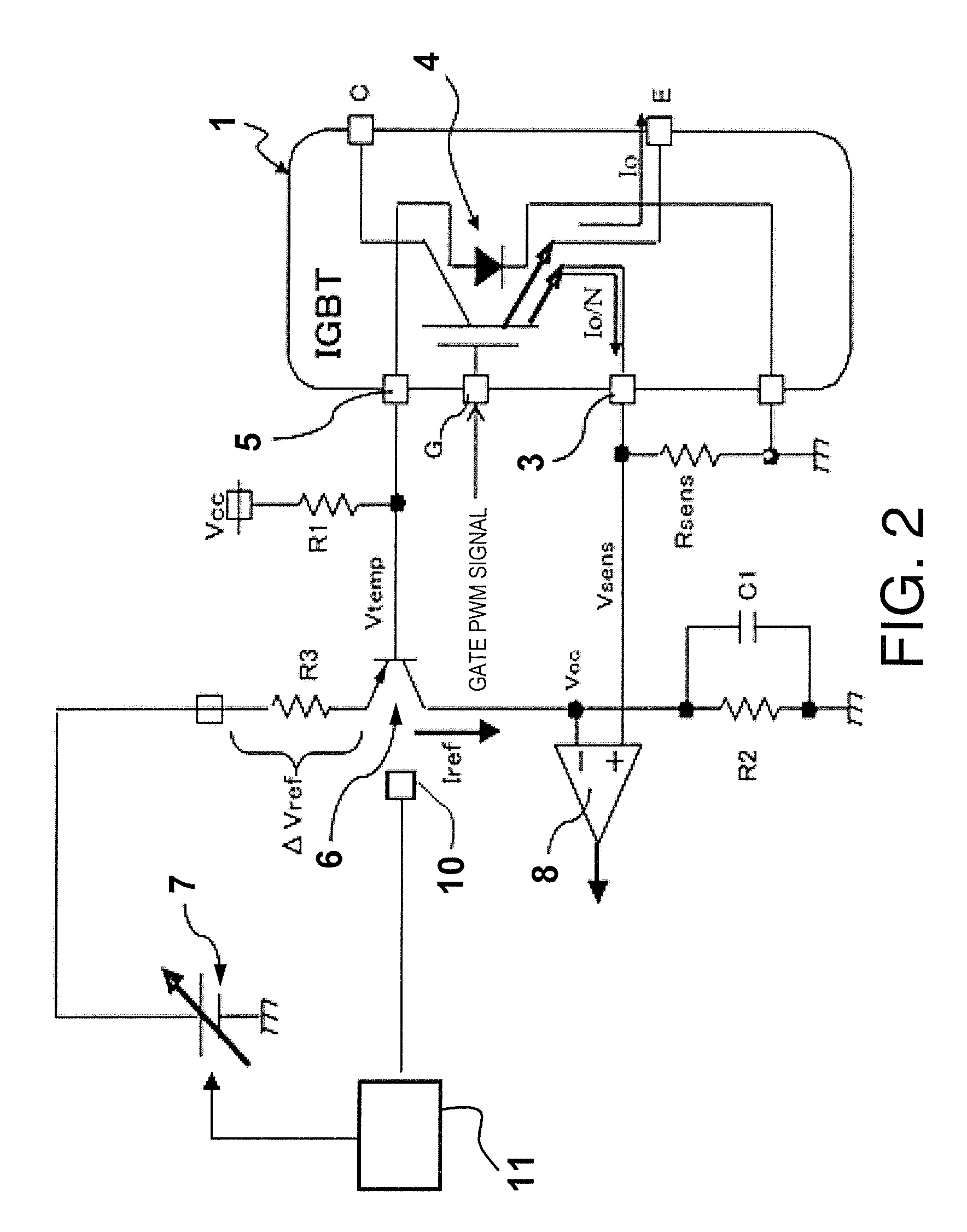
[0030]Referring now to FIG. 2, an over-current detecting apparatus in accordance with a second embodiment will now be explained. FIG. 2 is an electric circuit diagram showing the over-current detecting apparatus according to a second embodiment. In view of the similarity between the first and second embodiments, the parts of the second embodiment that are identical to the parts of the first embodiment will be given the same reference numerals as the parts of the first embodiment. Moreover, the descriptions of the parts of the second embodiment that are identical to the parts of the first embodiment may be omitted for the sake of brevity.
[0031]In the first embodiment, it is assumed that the voltage Vbe between the base and the emitter of the PNP transistor constituting the current converting element 6 does not depend on temperature, and thus, the base-emitter voltage Vbe does not appear in Equation 3. However, there are times when the base-emitter voltage Vbe of the current convertin...
third embodiment
[0033]Referring now to FIG. 3, an over-current detecting apparatus in accordance with a third embodiment will now be explained. In this embodiment, a current converting element 9 including a PNP transistor that is the same as current converting element 6 is used to reduce the effect of an ambient temperature of the current converting element 6. A base terminal of the current converting element 9 is connected to the reference power source 7, which has a small degree of temperature dependence, and an emitter terminal of the current converting element 9 is connected to the reference voltage point. The current converting element 9 is mounted on the same substrate as the current converting element 6.
[0034]In this embodiment, the previous Equation 2 can be revised to the Equation 2′ as shown below, where Vref is the voltage of the reference power source 7 and Vbe(9) is the voltage between the base and the emitter of the PNP transistor 9 connected to the power source 7.
Iref=((Vref+Vbe(9))−...
PUM
 Abstract
Description
Claims
Application Information


