
RF-power device

a power device and radio frequency technology, applied in the direction of fixed capacitor details, amplifiers with min 3 electrodes or 2 pn junctions, fixed capacitors, etc., can solve the problems of self-heating and mutual heating, large heat generation, performance degradation or even transistor damage, and achieve significant space saving and reduce mutual heating of rf-power transistors.

Inactive Publication Date: 2014-07-01
AMPLEON NETHERLANDS
View PDF8 Cites 0 Cited by
  • Summary
  • Abstract
  • Description
  • Claims
  • Application Information

AI Technical Summary

Benefits of technology

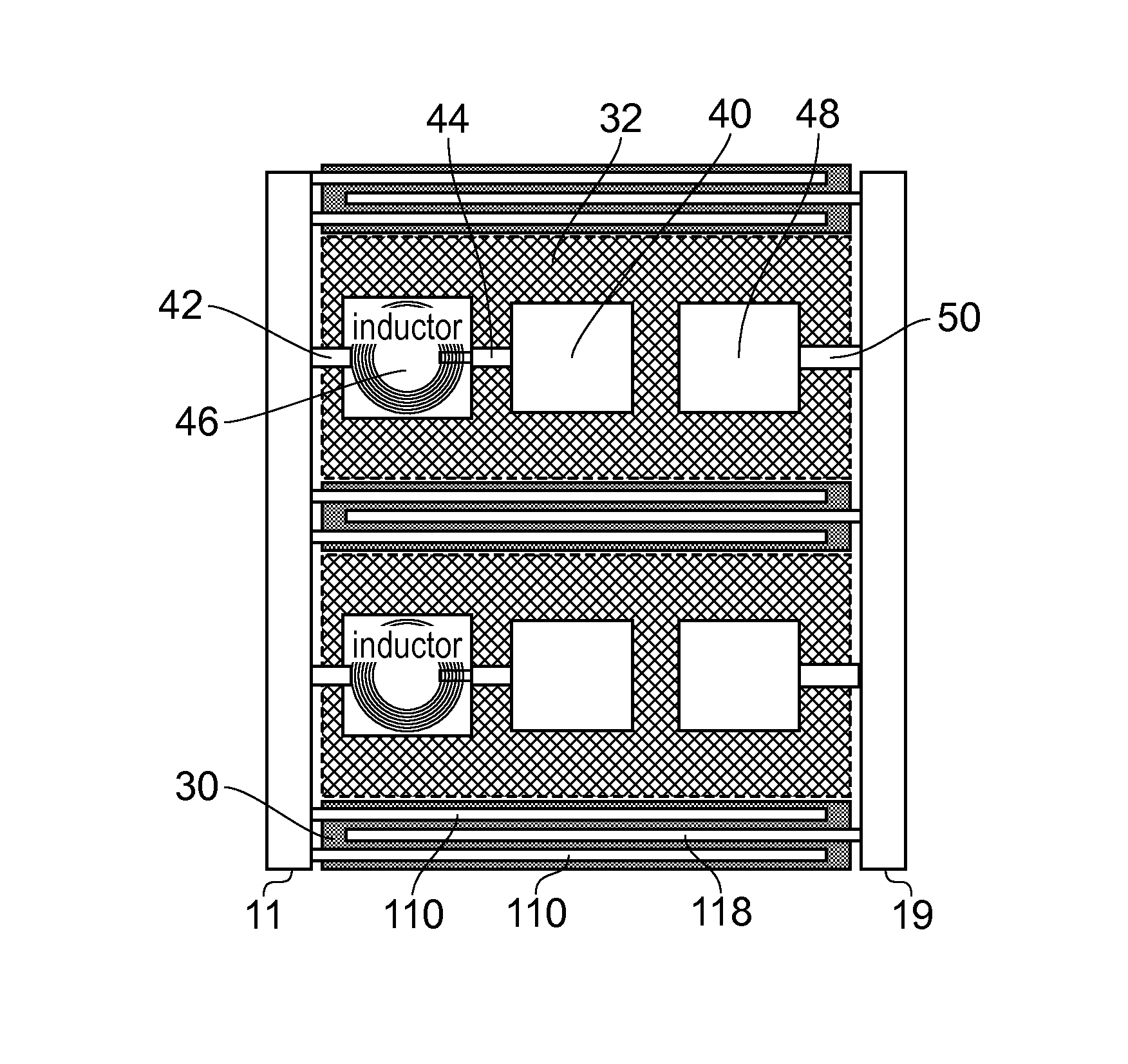
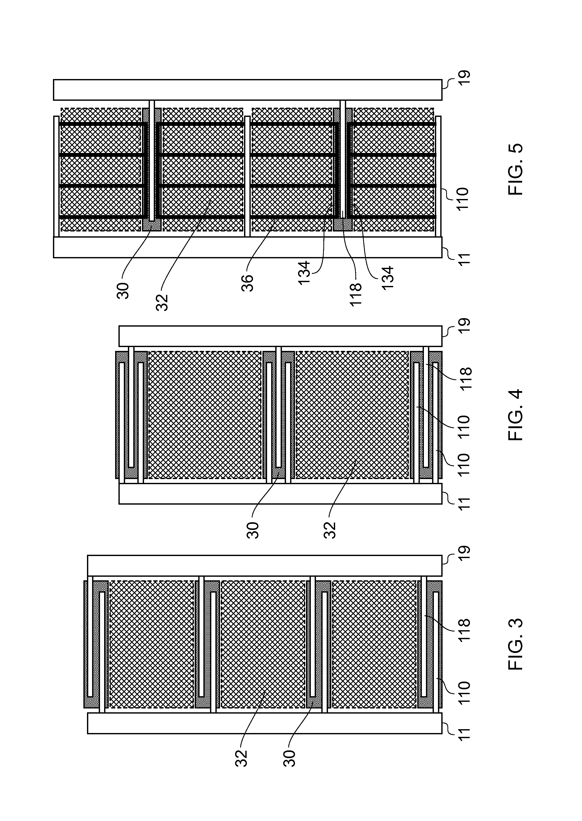
The invention is about a semiconductor substrate that has multiple active regions arranged in an array, each containing one or more RF-power transistors. These active regions are spaced apart from each other to reduce mutual heating. The substrate also includes impedance matching components in the inactive regions, which further help to reduce mutual heating. This design allows for more efficient use of space on the substrate compared to known designs where the impedance matching components are separate from the transistor array. Overall, this results in a significant space saving.

Problems solved by technology

Power devices of this kind generate a large amount of heat, which can lead to self heating and mutual heating between the devices in the array.
This heating can lead to performance degradation or even transistor damage.
The space in between the transistors represents a large amount dead space on the substrate in which the RF power device is provided.

Method used


Image

  • RF-power device
  • RF-power device
  • RF-power device

Examples


Embodiment Construction

[0024]Embodiments of the present invention are described in the following with reference to the accompanying drawings.

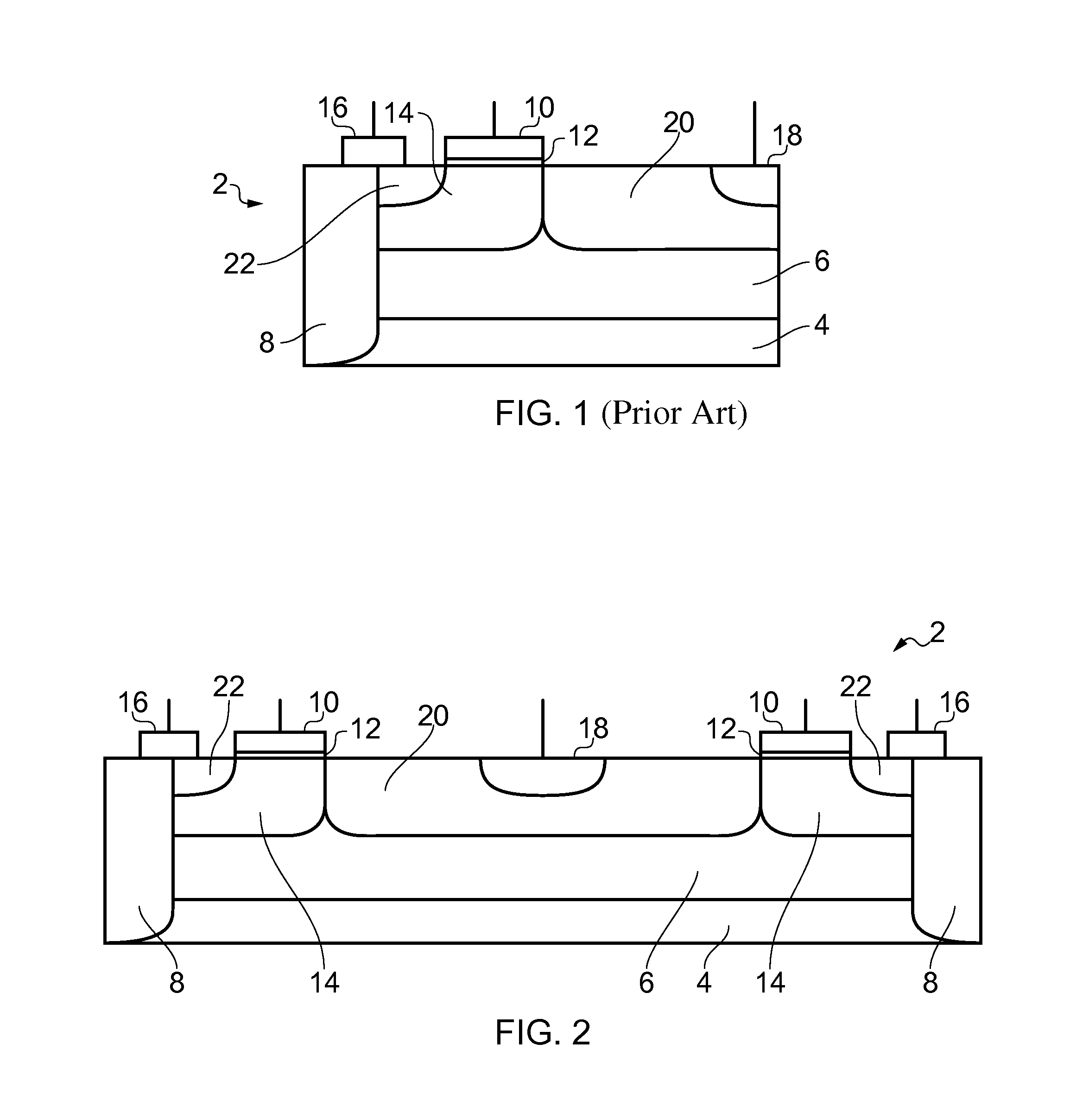
[0025]FIG. 1 shows a first example of an RF-power transistor 2. The RF-power transistor 2 is provided in a semiconductor substrate 4, and includes a source region 22 and a drain region 18. The source region 22 and the drain region 18 are provided in respective wells 14 and 20, which are formed in an epitaxial layer 6 on the substrate 4. The well 20 forms a drain drift region of the device. The well 14 forms a channel region of the device. As shown in FIG. 1, a contact 16 can be provided to connect to the source region 22 and the channel region of the well 14 to the substrate region 4 via a doped well region 8. Above the channel region in the well 14, there is provided a gate. The gate includes a dielectric 12 isolating a gate electrode 10 from the channel region.

[0026]This form of RF-power transistor is known in the art. Another version of this form of power transist...


PUM


Abstract

An RF-power device includes a semiconductor substrate having a plurality of active regions arranged in an array. Each active region includes one or more RF-power transistors. The active regions are interspersed with inactive regions for reducing mutual heating of the RF-power transistors in separate active regions. The devices also includes at least one impedance matching component located in one of the inactive regions of the substrate.

Description

CROSS-REFERENCE TO RELATED APPLICATIONS[0001]This application claims the priority under 35 U.S.C. §119 of European patent application no. 11150247.2, filed on Jan. 5, 2011, the contents of which are incorporated by reference herein.BACKGROUND OF THE INVENTION[0002]This invention relates to a radio frequency (RF) power device.[0003]It is known to provide RF power devices such as RF-LDMOS transistors and GaN-HEMT in an array on a semiconductor substrate.[0004]Power devices of this kind generate a large amount of heat, which can lead to self heating and mutual heating between the devices in the array. This heating can lead to performance degradation or even transistor damage.[0005]In an attempt to mitigate mutual heating of different transistors in the array, the transistors in known array designs are spaced apart by a given distance or pitch. The pitch used in practical devices is known to be 50-150 μm, whereas the size of the transistors themselves may be much smaller (e.g. 3-15 μm)....

Claims


Application Information

Patent Timeline
Patent Type & Authority Patents(United States)
IPC IPC(8): H03F3/68H01L23/50
CPCH01L2924/0002H01L23/66H01L27/0207H01L2924/00
Inventor WILLEMSEN, MARNIX, BERNARD
Owner AMPLEON NETHERLANDS
Learn More