

Structures and Methods of a Bistable Resistive Random Access Memory
a random access memory and bistable resistive technology, applied in the direction of semiconductor devices, electrical devices, transistors, etc., can solve the problems of manufacturing such devices with very small dimensions and the heat sink effect of conventional designs, and achieve the reduction of the amount of heat dissipation from the first conductor, and the reduction of the amount of heat dissipation from the second conductor
- Summary
- Abstract
- Description
- Claims
- Application Information
AI Technical Summary
Benefits of technology
Problems solved by technology
Method used
Image

Examples
first embodiment
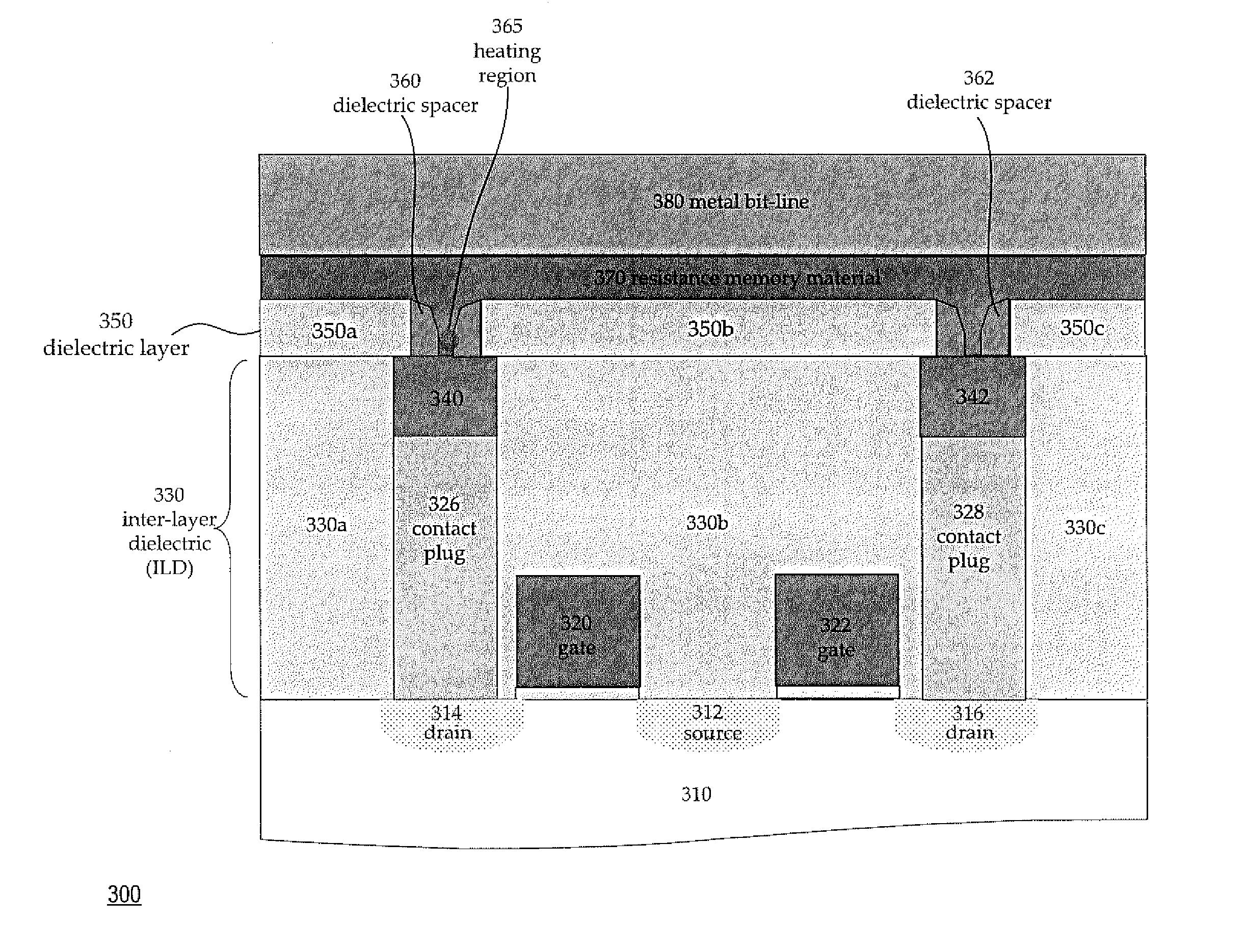
[0033] As depicted in FIG. 3, there is shown a process diagram illustrating a cross-sectional view of a bistable resistive random access memory 300 with an I-shaped structure of programmable resistive memory materials according to the present invention. The bistable resistive random access memory 300 is formed on a semiconductor substrate 310. Access transistors are formed by an n-type terminal 312 acting as a common source region and n-type terminals 314 and 316 acting as drain regions in the p-type substrate 310. Polysilicon word (gate) lines 320, 322 form the gates of the access transistors. An inter-layer dielectric 330 includes dielectric fills 330a, 330b and 330c where the dielectric fill 330b is formed over the polysilicon word lines 320, 322. The layer is patterned and conductive structures, including a common source line (not shown) and plug structures 326 and 328 are formed. The conductive material can be tungsten or other materials and combinations suitable for the plug a...
second embodiment
[0047]FIG. 9 is a cross-sectional view of a process diagram 900 illustrating the bistable resistive memory with the formation of a via. The dielectric layer 350 is deposited over the top surfaces of the inter-layer dielectric 330 and the programmable resistive memory materials 340, 342. In one embodiment, the dielectric layer 350 comprises silicon dioxide that is deposited using a chemical vapor deposition process. One property that the dielectric layer 350 possesses is the characteristic of low thermal conductivity. The etching of dielectric layer holes extends to a contact hole, which has a critical dimension that is the same or smaller than the contact hole. A relatively small via 910 has a critical dimension that is significantly less than the contact plug 326. The via 910 is patterned to land on the resistive memory material 340 in the contact plug 326. In one embodiment, the via 910 has a critical dimension ranging from about 10 nm to about 100 nm. The aspect ration of the via...
PUM
 Abstract
Description
Claims
Application Information