Electrically rewritable non-volatile memory element and method of manufacturing the same

a non-volatile memory element, electric rewritability technology, applied in the direction of electrical equipment, semiconductor devices, instruments, etc., can solve the problems of reducing the electrical power consumption of the device, dram is volatile memory that loses stored data, and the limit of the device, so as to reduce the size of the contact area between the recording layer and the upper electrode, reduce the amount of damage sustained, and improve the etching rate

Inactive Publication Date: 2007-03-22
ELPIDA MEMORY INC
View PDF5 Cites 166 Cited by
  • Summary
  • Abstract
  • Description
  • Claims
  • Application Information

AI Technical Summary

Benefits of technology

[0020] Another object of the present invention is to provide a non-volatile memory element comprising a recording layer that includes a phase change material, wherein thermal efficiency is increased in the non-volatile memory element by reducing the amount of heat released to the metal layer positioned above the recording layer while minimizing damage to the recording layer during manufacturing; and to provide a method for manufacturing the non-volatile memory element.
[0032] According to the present invention thus configured, the amount of heat released to the metal layer positioned above the recording layer is reduced in comparison with the conventional technique. The flow of the write current within the recording layer can also be further concentrated than in the conventional non-volatile memory element. The present invention thereby makes it possible to provide a non-volatile memory element having increased thermal efficiency, and to provide a method for manufacturing the same. Accordingly, not only can the write current be reduced, but the write speed can also be increased in comparison with the conventional technique. Since the protective insulation film is interposed between the interlayer insulation film and the upper surface of the recording layer, it becomes possible to reduce the amount of damage sustained by the recording layer during patterning of the recording layer and formation of the through-hole for exposing a portion of the recording layer.

Problems solved by technology

DRAM is volatile memory that loses stored data if its power supply is turned off.
That makes DRAM unsuitable for the storage of programs and archival information.
Also, even when the power supply is turned on, the device has to periodically perform refresh operations in order to retain stored data, so there are limits as to how much device electrical power consumption can be reduced, while yet a further problem is the complexity of the controls run under the controller.
Semiconductor flash memory is high capacity and non-volatile, but requires high current for writing and erasing data, and write and erase times are slow.
These drawbacks make flash memory an unsuitable candidate for replacing DRAM in main memory applications.
There are other non-volatile memory devices, such as magnetoresistive random access memory (MRAM) and ferroelectric random access memory (FRAM), but they cannot easily achieve the kind of storage capacities that are possible with DRAM.
However, since the entire upper surface of the recording layer composed of the phase change material is in contact with a metal layer in the non-volatile memory element described in “Scaling Analysis of Phase-Change Memory Technology,” A. Pirovano, A. L. Lacaita, A. Benvenuti, F. Pellizzer, S. Hudgens, and R. Bez, IEEE 2003, the heat generated when the write current is applied is easily released to the side of the metal layer, creating drawbacks of low thermal efficiency.
Reduced thermal efficiency leads to increased power consumption and increased write times.
The requirement that the upper electrode be composed of a conductive material makes it difficult to significantly reduce the coefficient of thermal conductivity of the upper electrode itself.
Since the write current flows in scattered fashion when the entire upper surface of the recording layer is in contact with the upper electrode, it is difficult to adequately increase thermal efficiency.
It is therefore impossible to reduce the amount of heat released to the metal layer positioned above the recording layer.
The non-volatile memory elements described in above three papers and U.S. Pat. No. 5,536,947 thus have drawbacks in having low thermal efficiency due to the large amount of heat released to the metal layer positioned above the recording layer.
However, in the non-volatile memory elements described in Japanese Patent Application Laid Open Nos. 2004-289029 and 2004-349709, there is a risk of the recording layer being significantly damaged during patterning of the recording layer, or during formation of a through-hole for exposing a portion of the recording layer.
However, the upper electrode cannot be made to function as a protective film in the case of a structure in which only a portion of the upper surface of the recording layer is in contact with the upper electrode, such as in the non-volatile memory elements described in Japanese Patent Application Laid Open Nos. 2004-289029 and 2004-349709.
There is therefore a risk of significant damage to the recording layer occurring during patterning of the recording layer or formation of the through-hole, as described above.

Method used


Image

  • Electrically rewritable non-volatile memory element and method of manufacturing the same
  • Electrically rewritable non-volatile memory element and method of manufacturing the same
  • Electrically rewritable non-volatile memory element and method of manufacturing the same

Examples


first embodiment

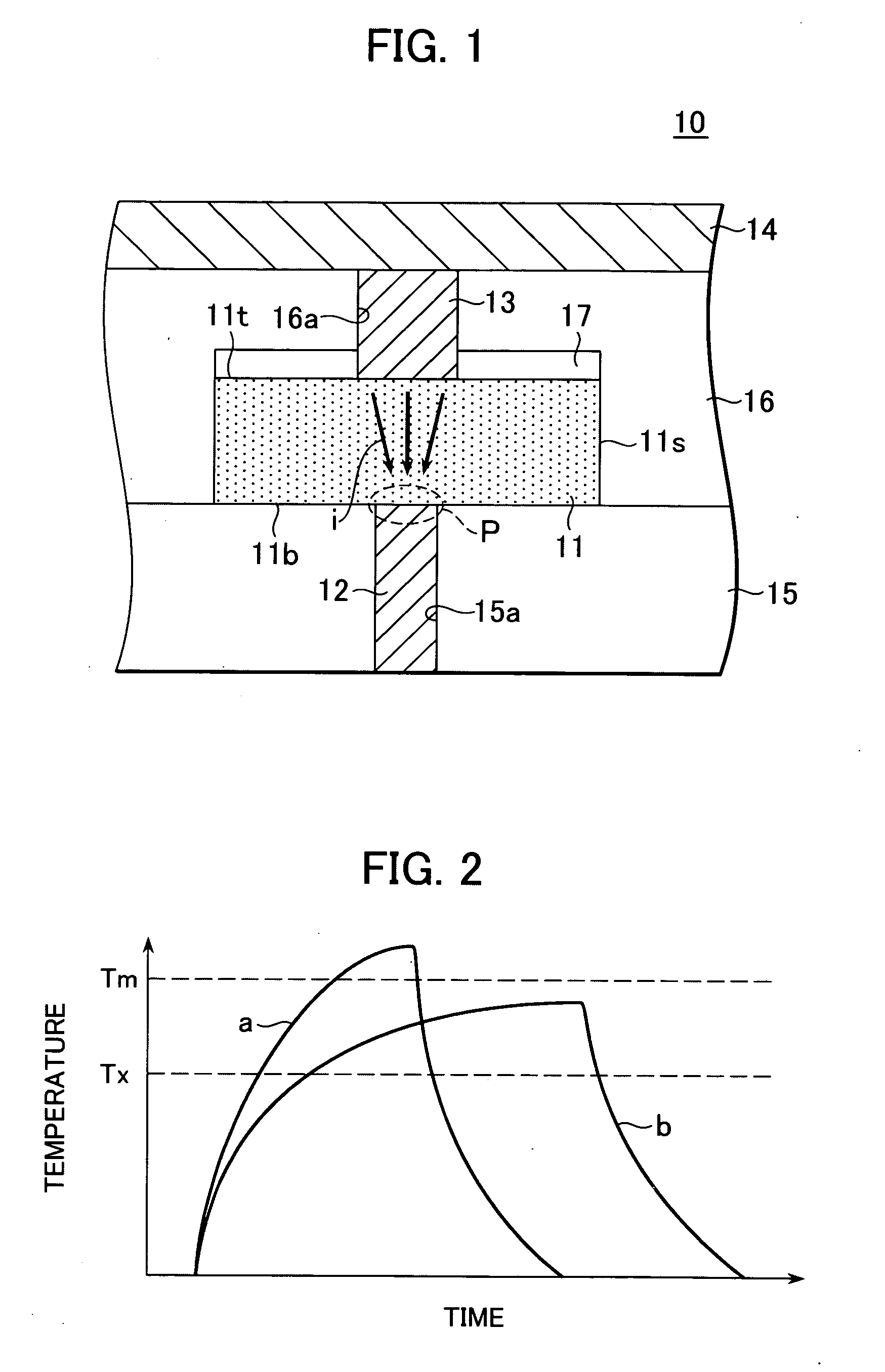
[0097] This type of configuration makes it possible to even further decrease the amount of heat released to the side of the upper electrode 13, since the heat capacity of the upper electrode 13 decreases. A level of thermal efficiency higher than that of the first embodiment can thereby be obtained, and it becomes possible not only to further decrease the write current, but also to further increase the write speed.

[0098] The method for manufacturing the non-volatile memory element 20 according to the present embodiment will next be described.

[0099]FIG. 8 is a schematic sectional view showing the sequence of steps for manufacturing the non-volatile memory element 20.

[0100] By performing the same steps as those described using FIGS. 5 and 6, a through-hole 16a is formed in the second interlayer insulation film 16, after which the upper electrode 13 is formed with a thickness sufficient to fill a portion of the through-hole 16a as shown in FIG. 8. A buried member 21 is then formed wi...

fifth embodiment

[0113] The non-volatile memory element 50 according to a preferred fifth embodiment of the present invention will next be described.

[0114]FIG. 15 is a schematic sectional view showing the structure of the non-volatile memory element 50 according to a fifth preferred embodiment of the present invention.

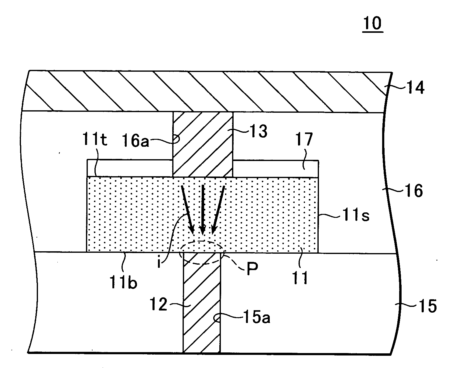
[0115] As shown in FIG. 15, the non-volatile memory element 50 according to the present embodiment differs from the non-volatile memory element 10 according to the first embodiment in that sidewalls 51 are formed in the inner wall of the through-hole 16a, and the upper electrode 13 is provided in the region 51a surrounded by the sidewalls 51. Since other aspects of this configuration are the same as in the non-volatile memory element 10 according to the first embodiment, the same reference symbols are used to indicate the same elements, and descriptions of these elements are not repeated.

[0116] The sidewalls 51 are not subject to any particular limitations insofar as they are compose...


PUM


Abstract

A non-volatile memory element includes a recording layer that includes a phase change material, a lower electrode provided in contact with the recording layer, an upper electrode provided in contact with a portion of the upper surface of the recording layer, a protective insulation film provided in contact with the other portion of the upper surface of the recording layer, and an interlayer insulation film provided on the protective insulation film. High thermal efficiency can thereby be obtained because the size of the area of contact between the recording layer and the upper electrode is reduced. Providing the protective insulation film between the interlayer insulation film and the upper surface of the recording layer makes it possible to reduce damage sustained by the recording layer during patterning of the recording layer or during formation of the through-hole for exposing a portion of the recording layer.

Description

TECHNICAL FIELD [0001] The present invention relates to an electrically rewritable non-volatile memory element and to a method of manufacturing the element. More specifically, the present invention relates to an electrically rewritable non-volatile memory element having a recording layer that includes phase change material, and to a method of manufacturing the element. BACKGROUND OF THE INVENTION [0002] Personal computers and servers and the like use a hierarchy of memory devices. There is lower-tier memory, which is inexpensive and provides high storage capacity, while memory higher up the hierarchy provides high-speed operation. The bottom tier generally consists of magnetic storage such as hard disks and magnetic tape. In addition to being non-volatile, magnetic storage is an inexpensive way of storing much larger quantities of information than solid-state devices such as semiconductor memory. However, semiconductor memory is much faster and can access stored data randomly, in co...

Claims


Application Information

Patent Timeline
Patent Type & Authority Applications(United States)
IPC IPC(8): H01L29/04
CPCG11C2213/52H01L27/2436H01L45/06H01L45/1233H01L45/126H01L45/1683H01L45/143H01L45/144H01L45/148H01L45/1675H01L45/1273H10B63/30H10N70/8413H10N70/8418H10N70/231H10N70/8825H10N70/884H10N70/8828H10N70/826H10N70/063H10N70/066
Inventor ASANO, ISAMUSATO, NATSUKINAKAI, KIYOSHI
Owner ELPIDA MEMORY INC
Why Eureka
Try Eureka