Multidimensional Structural Access

a multi-dimensional, microscopic technology, applied in the testing/measurement of individual semiconductor devices, semiconductor/solid-state devices, instruments, etc., can solve the problems of difficult to measure, analyze and locate faults in 3d microscopic (including nanoscopic) structures, or the final access to the voi is either more complicated or impossible, so as to minimize the damage to the region

Active Publication Date: 2015-09-17
FEI CO
View PDF12 Cites 57 Cited by
  • Summary
  • Abstract
  • Description
  • Claims
  • Application Information

AI Technical Summary

Benefits of technology

[0009]Multiple planes within the sample are exposed from a single perspective for imaging and / or probing. For example, the sample can be milled at a non-orthogonal angle to expose different layers as sloped surfaces. The non-orthogonal milling exposes edges of multiple, parallel conductor planes to provide access to multiple levels from above. Once exposed, the planes can be accessed, for example, for contacting with an electrical probe for applying or sensing a voltage. The level of an exposed layer to be contacted can be identified, for example, by counting down the exposed layers from the sample surface, since the non-orthogonal mill makes all layers visible from above. Alternatively, the sample can be milled orthogonally to the surface, and then tilted and / or rotated to provide access to multiple levels of the device. The milling is preferably performed away from the region of interest, to provide electrical access to the region while minimizing damage to the region.

Problems solved by technology

It is difficult to measure, analyze and locate faults in 3D microscopic (including nanoscopic) structures.
For 3D IC structures, prior art techniques that provide planar access are inherently limited to two dimensions of the structure, resulting in either more complicated or impossible final access to the VOI.

Method used


Image

  • Multidimensional Structural Access
  • Multidimensional Structural Access
  • Multidimensional Structural Access

Examples


Embodiment Construction

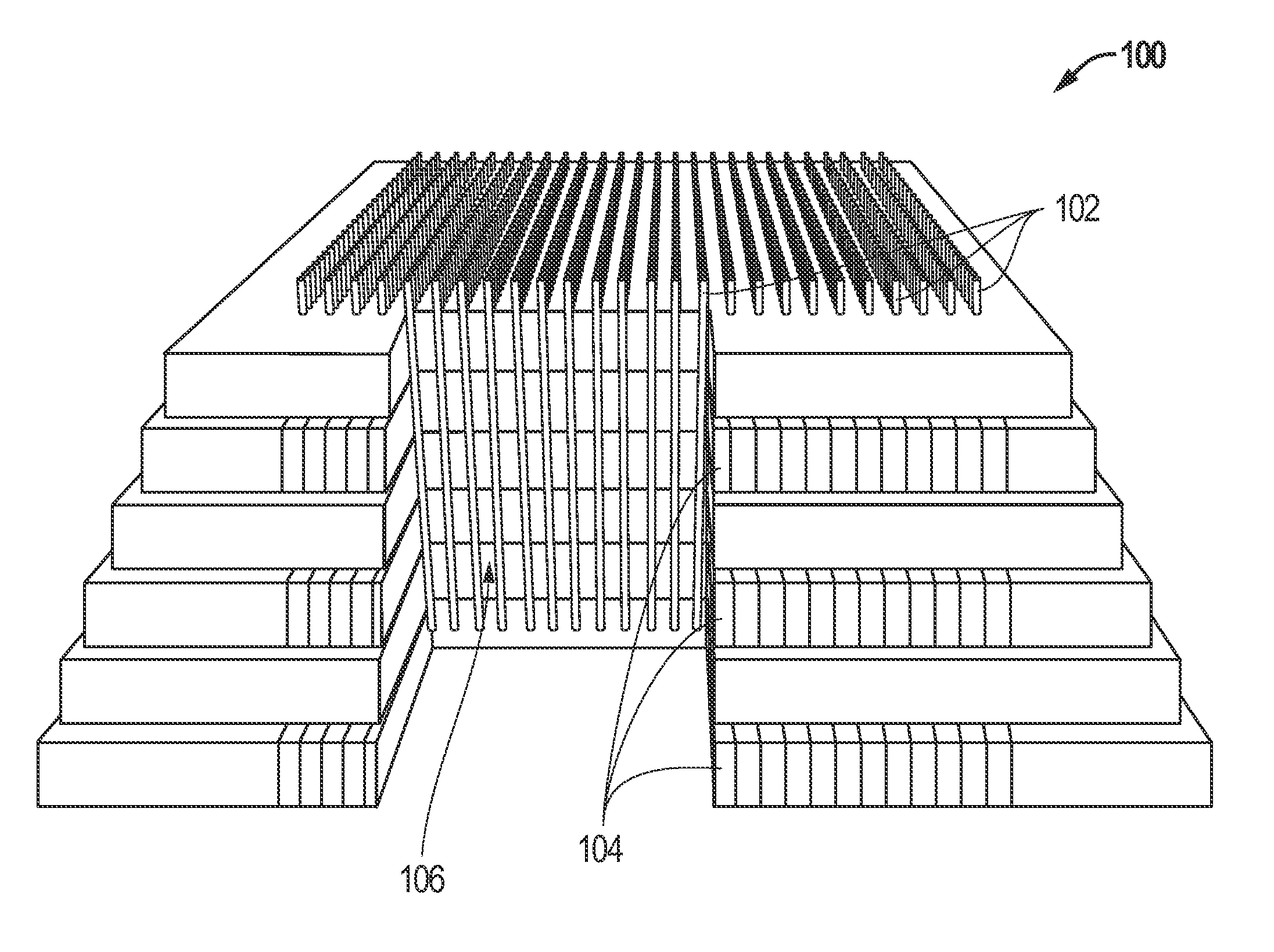
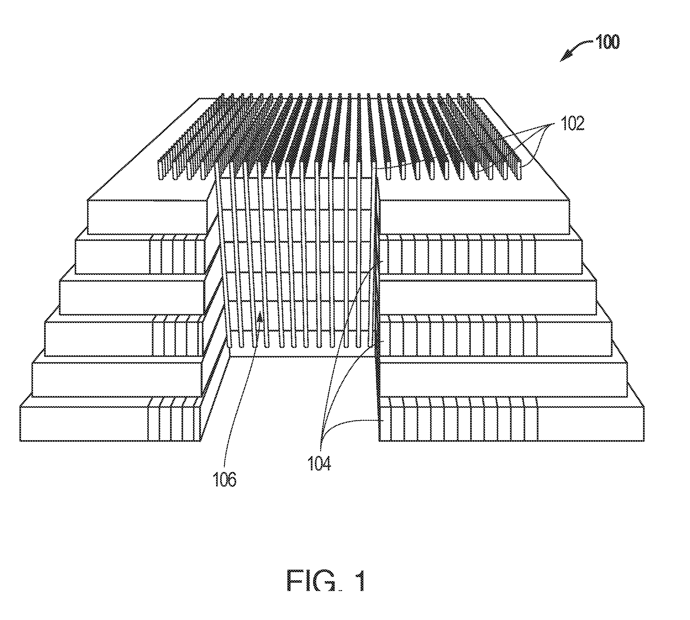
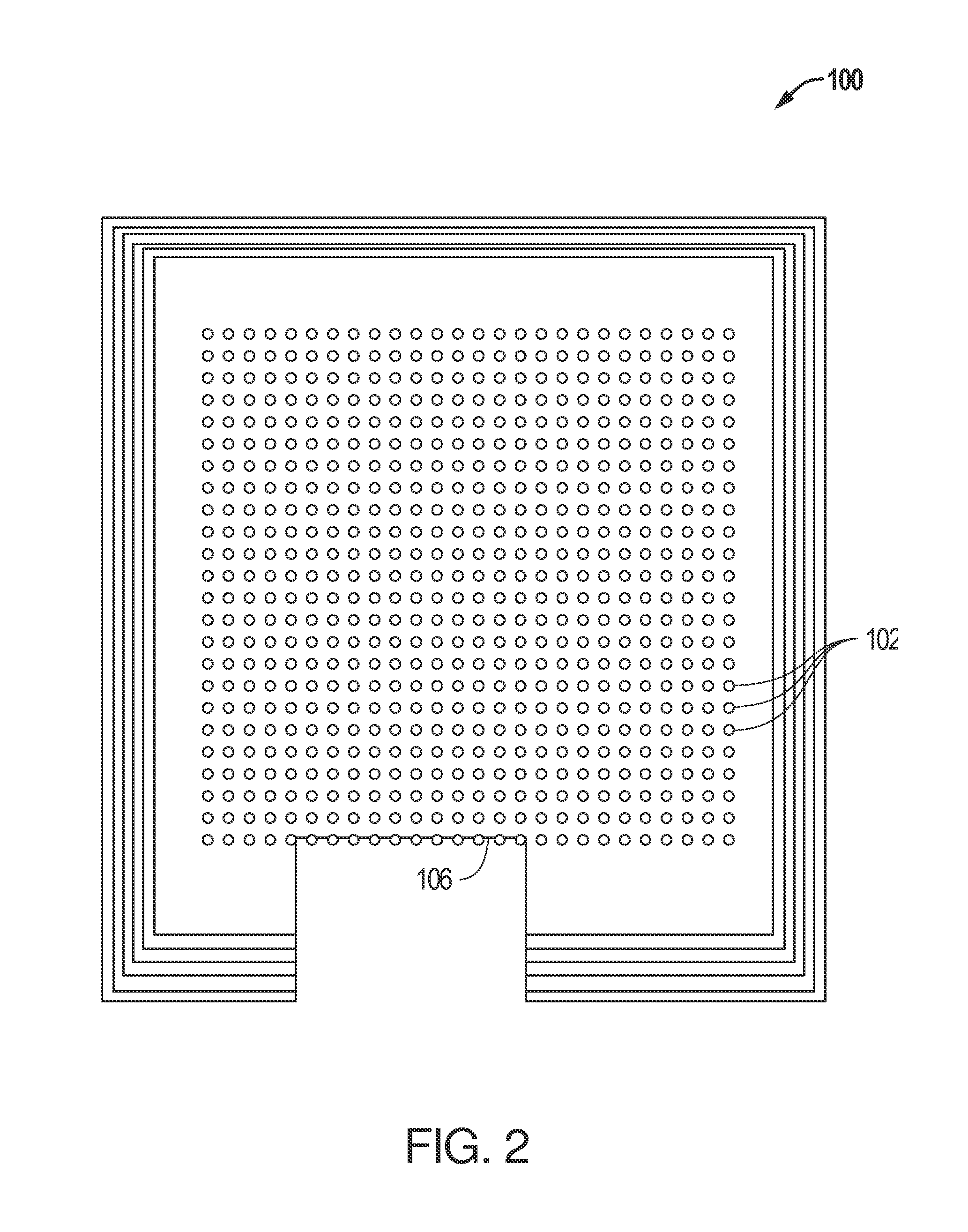
[0020]In one conventional analysis of two-dimensional processing, a region of interest is exposed by ion beam milling and electrical probes are contacted to the region of interest, typically from above. The region of interest can be viewed from above using an electron beam with voltage applied for voltage contrast imaging. This works well for 2D structures, but for newer structures having transistors or memory cells on many layers, it is very difficult to access the correct layer in the stack when one is looking at the structure from the top. In accordance with an aspect of some embodiments of the invention, the sample is milled and / or tilted so that multiple planes within the sample are exposed from a single perspective, typically from above, for imaging or probing.

[0021]Also, most prior art cross-sectional techniques are preformed through the region of interest, such as the particular failing part in a failure analysis. Due to the increased complexity of new 3D structures it is ad...


PUM


Abstract

Multiple planes within the sample are exposed from a single perspective for contact by an electrical probe. The sample can be milled at a non-orthogonal angle to expose different layers as sloped surfaces. The sloped edges of multiple, parallel conductor planes provide access to the multiple levels from above. The planes can be accessed, for example, for contacting with an electrical probe for applying or sensing a voltage. The level of an exposed layer to be contacted can be identified, for example, by counting down the exposed layers from the sample surface, since the non-orthogonal mill makes all layers visible from above. Alternatively, the sample can be milled orthogonally to the surface, and then tilted and / or rotated to provide access to multiple levels of the device. The milling is preferably performed away from the region of interest, to provide electrical access to the region while minimizing damage to the region.

Description

TECHNICAL FIELD OF THE INVENTION[0001]The present invention relates to processing of multidimensional, microscopic structures to provide electrical access to internal structures.BACKGROUND OF THE INVENTION[0002]As semiconductor fabrication processes pack more circuitry into smaller packages, integrated circuit (IC) designs are becoming more three-dimensional (3D). It is difficult to measure, analyze and locate faults in 3D microscopic (including nanoscopic) structures.[0003]An engineer will typically identify a region-of-interest (ROI) that he wants to investigate, based upon, for example, aberrant electrical behavior of a circuit component. Most ROIs in conventional ICs are confined to a small volume of the device in a planar region. For example, a static random access memory (SRAM) or a conventional “not-and” (NAND) flash cell each occupies a distinct X and Y location, with a small volume of active area in the Z direction. An engineer typically identifies the ROI by starting with ...

Claims


Application Information

Patent Timeline
Patent Type & Authority Applications(United States)
IPC IPC(8): G01R31/265H01J37/153
CPCH01J37/153G01R31/2653G01N1/286G01N1/32G01R31/306H01J37/3005H01L22/14H01J2237/208H01J2237/24564H01J2237/2817H01J2237/31749H01L2924/0002G01R31/2808G01R31/312G01R31/2898H01L2924/00G01R31/307
Inventor BLACKWOOD, JEFFREYLEE, SANG HOONSCHMIDT, MICHAELSTONE, STACEYHOLLAND, KAREY
Owner FEI CO
Why Eureka
Try Eureka