SD/SDIO host controller

a host controller and controller technology, applied in the field of host controllers, can solve the problems of lack of flexibility, inability to guarantee the timing characteristics of the register, and prone to be limited

Active Publication Date: 2014-07-08
OMNIVISION TECH (SHANGHAI) CO LTD
View PDF7 Cites 0 Cited by
  • Summary
  • Abstract
  • Description
  • Claims
  • Application Information

AI Technical Summary

Benefits of technology

[0009]In order to solve the problem encountered by the prior art, the main purpose of the present invention is to provide an SD / SDIO host controller which is capable of solving the setup / hold time issues caused by delay in digital signals and preventing phase deviation generated from a chip internal delay or a delay in the circuit of the test board.
[0017]Compared with the prior art, the SD / SDIO host controller of the present invention employs a frequency divider to perform frequency division on a local high-speed clock so as to obtain the operating clock of the SD / SDIO card, and simultaneously generates a trigger / sampling enable signal by the frequency divider and enables the position of the enable signal to be adjustable with respect to the operating clock of the SD / SDIO card. In this way, the setup / hold time issues caused by delay in digital signals can be solved through adjusting the position of the enable signal to extend Tset or Thold.

Problems solved by technology

1) When testing and verifying by using FPGAs (Field-Programmable Gate Array), the stability of timing characteristics can only be guaranteed by employing a trigger using the global clock network, and therefore, if a register is directly triggered by the clock returned from the chip pin, the timing characteristics of the register will not be guaranteed and setup / hold timing violations may occur, which will be reflected as instability during the test.
2) When implementing by using ASICs (Application Specific Integrated Circuit), both signal delay from the register's Q-end to the chip pins and signal delay from the chip pins to the register's D-end must be accurately controlled so as to obtain a satisfying setup / hold time.
3) Sampling locations are not adjustable, leading to the lack of flexibility and the proneness to be limited by a delay in the circuit of the test board.
Thus, it is clear that fixed trigger / sampling points will be affected by signal delay.
However, as trigger / sampling points cannot be flexibly arranged at the end of SD / SDIO cards, the setup / hold time issues caused by signal delay are mostly solved through accurately controlling the chip internal delay, thus resulting in a number of limitations.

Method used


Image

  • SD/SDIO host controller
  • SD/SDIO host controller
  • SD/SDIO host controller

Examples


Embodiment Construction

[0023]The present invention will be described and specified below with reference to specific exemplary examples in combination with accompanying drawings. Other advantages and effects of the present invention will be easily understood by those skilled in this art based on the disclosure contained in the specification. The present invention is applicable to other embodiments or of being practiced or carried out in various ways, and variations and modifications may be made in details of the specification on the condition of different views and applications without departing from the spirit of the invention.

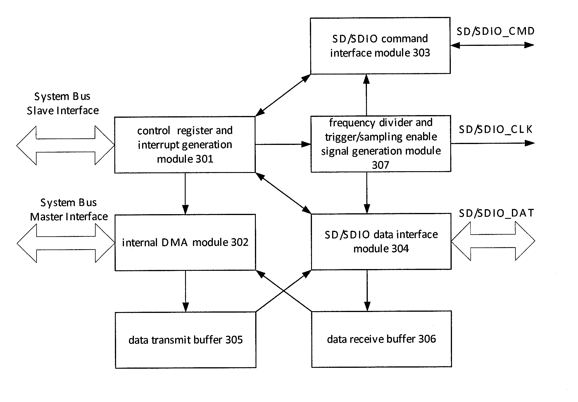
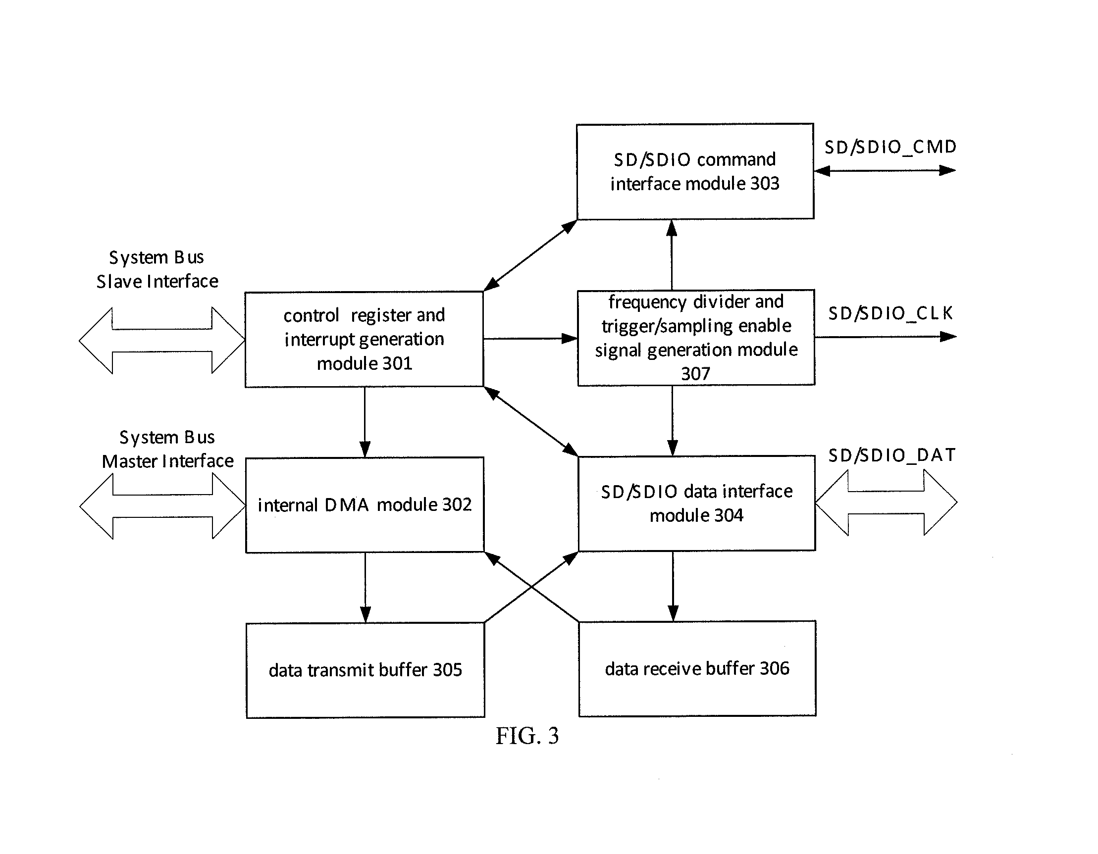
[0024]FIG. 3 is a block diagram illustrating the architecture of an SD / SDIO host controller in a preferred embodiment of the present invention. Referring to FIG. 3, the SD / SDIO host controller of the present invention includes a control register and interrupt generation module 301, an internal DMA module 302, an SD / SDIO command interface module 303, an SD / SDIO data interface module ...


PUM


Abstract

An SD / SDIO host controller is disclosed, which includes a control register and interrupt generation module, an internal DMA module, an SD / SDIO command interface module, an SD / SDIO data interface module, and a frequency divider and trigger / sampling enable signal generation module which is connected to an output end of the control register and interrupt generation module; the frequency divider and trigger / sampling enable signal generation module employs a frequency divider to perform frequency division on a local high-speed clock so as to obtain the operating clock of the SD / SDIO card, and simultaneously generates a trigger / sampling enable signal by the frequency divider and enables the position of the enable signal to be adjustable with respect to the operating clock of the SD / SDIO card. The present invention is capable of solving the setup / hold time issues caused by delay in digital signals.

Description

CROSS-REFERENCE TO RELATED APPLICATIONS[0001]This application claims the priority of Chinese patent application number 201110321380.5, filed on Oct. 20, 2011, the entire contents of which are incorporated herein by reference.TECHNICAL FIELD[0002]The present invention relates to a host controller, and more particularly, to an SD / SDIO host controller.BACKGROUND[0003]The most common practice of the prior art in data signal triggering / sampling is to use a clock returned from a chip pin to trigger / sample the data signal, but this method has three shortcomings as follows:[0004]1) When testing and verifying by using FPGAs (Field-Programmable Gate Array), the stability of timing characteristics can only be guaranteed by employing a trigger using the global clock network, and therefore, if a register is directly triggered by the clock returned from the chip pin, the timing characteristics of the register will not be guaranteed and setup / hold timing violations may occur, which will be reflect...

Claims


Application Information

Patent Timeline
Patent Type & Authority Patents(United States)
IPC IPC(8): G06F13/28G06F5/00G06F13/00
CPCG06F13/4291
Inventor ZHENG, YUCHICHEN, JINXIANG
Owner OMNIVISION TECH (SHANGHAI) CO LTD
Why Eureka
Try Eureka