

Page buffer circuit
a buffer circuit and page technology, applied in the field of page buffers, can solve problems such as unfavorable memory cell programming
- Summary
- Abstract
- Description
- Claims
- Application Information
AI Technical Summary
Benefits of technology
Problems solved by technology
Method used
Image

Examples
Embodiment Construction
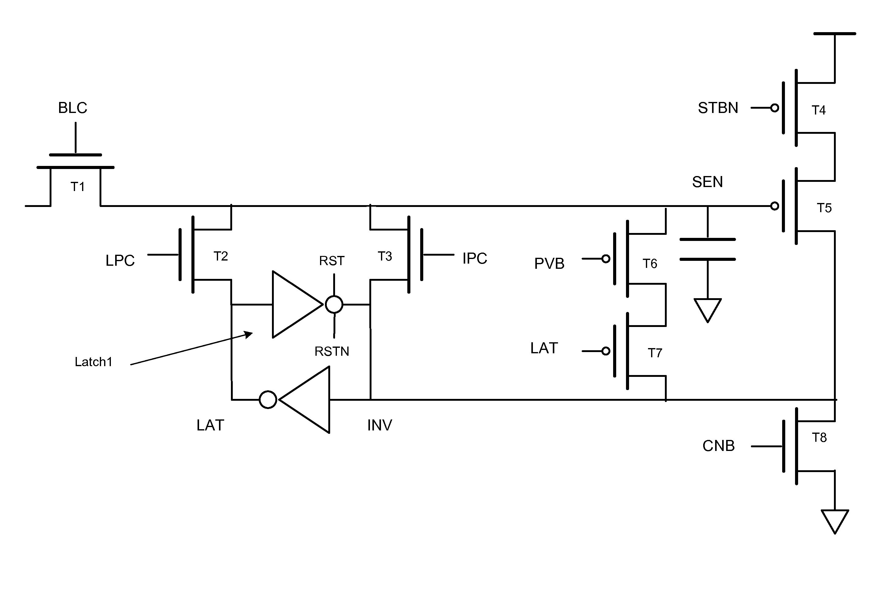
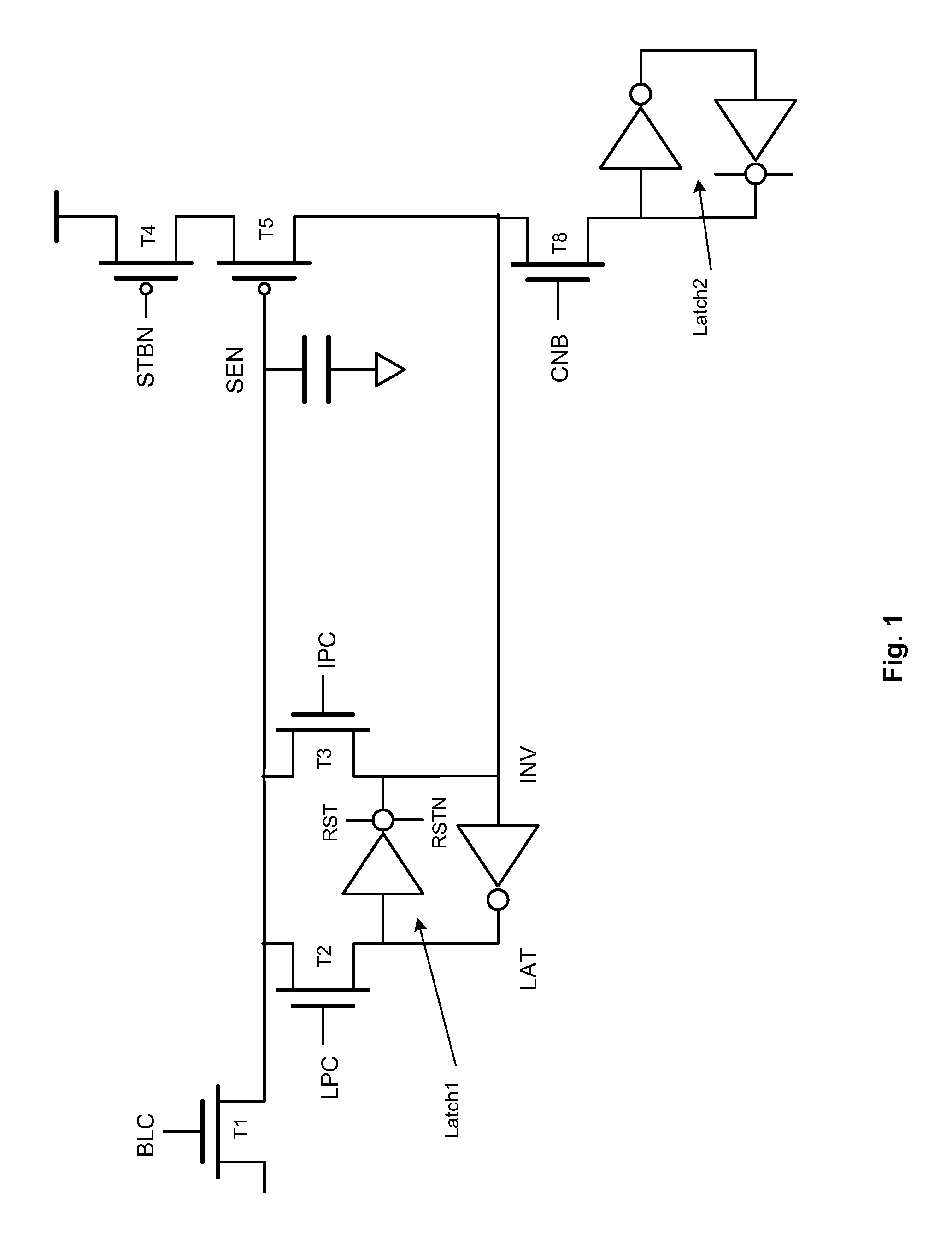
[0030]FIG. 1 is a circuit diagram of a page buffer circuit with multiple latches to store data.
[0031]Transistor T1 is an n-type MOSFET controlled by signal BLC at the gate of transistor T1. Depending on signal BLC, transistor T1 connects or disconnects a bit line (not shown) and node SEN. The bit line and node SEN are connected to a source and a drain of transistor T1.
[0032]Node SEN has a capacitance as shown. Node SEN is connected to the gate of transistor T5, a p-type MOSFET. A drain of transistor T5 is connected to node INV of Latch1, discussed below.
[0033]Transistor T5 is connected in series with transistor T4, a p-type MOSFET. Transistor T4 connects a supply voltage with transistor T5. A source of transistor T4 is coupled to the supply voltage and a drain of transistor T4 is coupled to a source of transistor T5. A gate of transistor T4 connected to signal STBN.
[0034]Latch1 has two inverters cross-coupled such that the output of one is connected to the input of the other. Latch ...
PUM
 Abstract
Description
Claims
Application Information