Page buffer circuit of flash memory device and program operation method thereof

a buffer circuit and flash memory technology, applied in the field of flash memory devices, can solve problems such as failure in program operation, and achieve the effect of reducing program failur

Inactive Publication Date: 2007-08-09
SK HYNIX INC
View PDF3 Cites 8 Cited by
  • Summary
  • Abstract
  • Description
  • Claims
  • Application Information

AI Technical Summary

Benefits of technology

[0010]An embodiment of the present invention provides a page buffer circuit of a flash memory device, which can reduce the program failure by re-verifying a memory cell during the next verification process.

Problems solved by technology

This may be caused by noise, etc. within the page buffer circuit 10.
Accordingly, failure occurs in the program operation.

Method used


Image

  • Page buffer circuit of flash memory device and program operation method thereof
  • Page buffer circuit of flash memory device and program operation method thereof
  • Page buffer circuit of flash memory device and program operation method thereof

Examples


Embodiment Construction

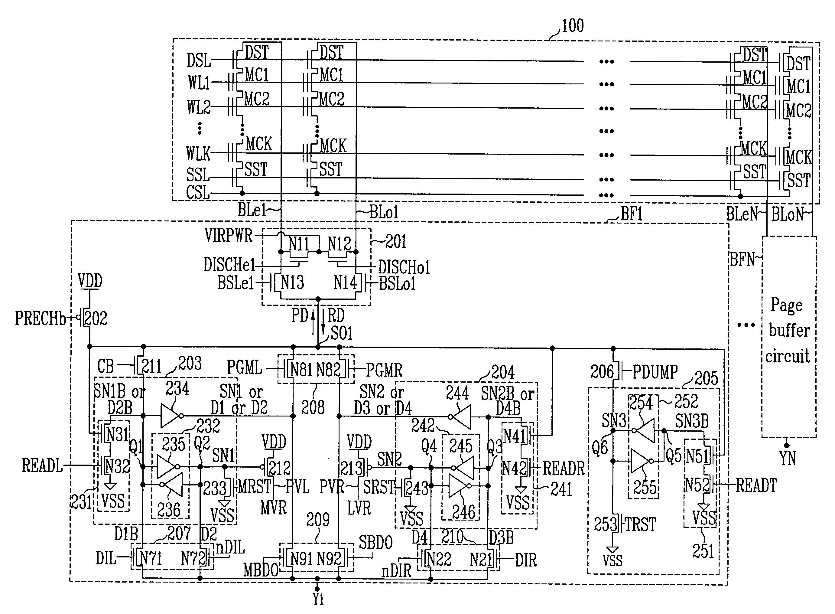
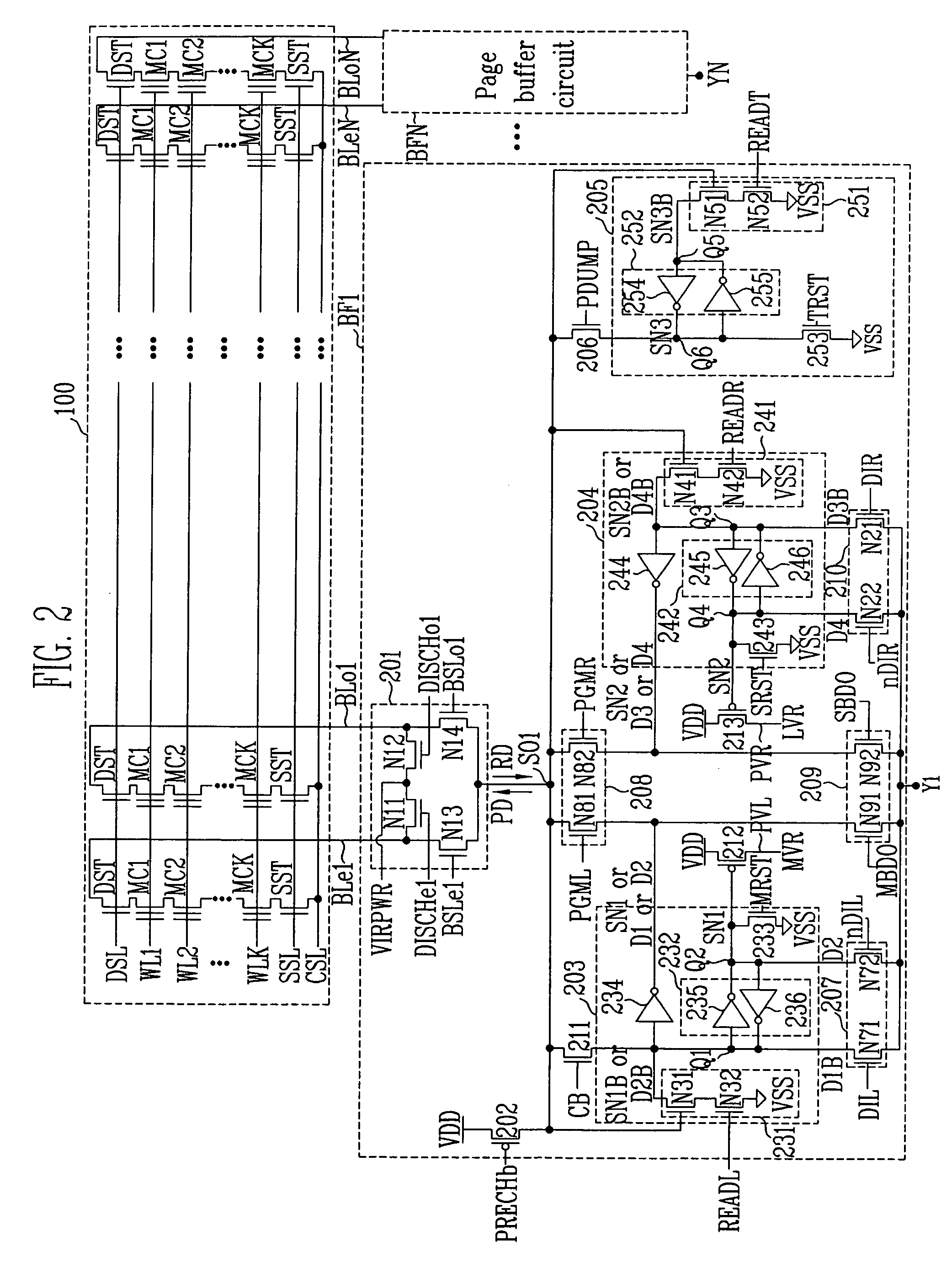
[0021]Referring to FIG. 2, a memory cell array 100 includes memory cells MC1 to MCK (K is an integer) that share bit lines BLe1 to BLeN, BLo1 to BLoN (N is an integer) and word lines WL1 to WLK. The memory cells MC1 to MCK may include single-level cells capable of storing 1-bit or multi-level cells capable of storing 2-bits. The memory cell array 100 further includes drain select transistors DST controlled by a drain select line DSL and source select transistors SST controlled by a source select line SSL. Memory cells connected to the same word line (e.g., WL1) form one page. The construction and operation of the memory cell array 100 are well known to those having ordinary skill in the art and the description thereof will be omitted.

[0022]Each of page buffers BF1 to BFN (N is an integer) is connected to a pair of bit lines. For example, the page buffer BF1 may be connected to the bit lines BLe1, BLo1. Since page buffers BF1 to BFN have substantially the same construction and operat...


PUM


Abstract

A page buffer circuit includes a bit line selection circuit, a main register, a program transmission circuit, a temporary register, and a verification transmission circuit. The verification transmission circuit transmits data stored in the temporary register to the main register through a sensing node in response to a transmission control signal during a program verification operation. A memory cell that has been determined to be programmed in a previous program verification process is verified again in a next program verification process.

Description

BACKGROUND[0001]The present invention relates to flash memory devices, and more particularly to a page buffer circuit and a program operation method.[0002]In general, the read and program operations of a flash memory device are executed one page at time using a page buffer circuit. The construction and operation of the page buffer circuit in the related art will be described below.[0003]FIG. 1 is a schematic circuit diagram of a page buffer circuit of a flash memory device in the related art. A page buffer circuit 10 includes a bit line selection circuit 11, a precharge circuit 12, a first register 13, a second register 14, a data input circuit 15, a data transmission circuit 16, a data output circuit 17, a first verification circuit 18, and a second verification circuit 19. The first register 13 includes a first sensing circuit 31, a first latch circuit 32, and a first reset circuit 33. The second register 14 includes a second sensing circuit 41, a second latch circuit 42, and a se...

Claims


Application Information

Patent Timeline
Patent Type & Authority Applications(United States)
IPC IPC(8): G11C14/00G11C7/10G11C11/34G11C16/06
CPCG11C7/1021G11C16/3459G11C16/3454G11C16/24A46B5/026A46D1/0238A46D1/006A46B9/08A46B2200/106
Inventor CHUNG, JUN SEOP
Owner SK HYNIX INC
Why Eureka
Try Eureka