Semiconductor memory device and related programming method

a memory device and semiconductor technology, applied in the field of semiconductor memory devices, can solve the problems of increasing voltage applied to the various connected source lines, rams are volatile memory devices that lose their stored data, and flash memory cells that do not allow current to flow, so as to prevent the inadvertent elevation of wordline voltage and negative effects

Active Publication Date: 2008-09-16
SAMSUNG ELECTRONICS CO LTD
View PDF13 Cites 10 Cited by
  • Summary
  • Abstract
  • Description
  • Claims
  • Application Information

AI Technical Summary

Problems solved by technology

RAMs are volatile memory devices that lose their stored data when power is interrupted.
In this condition, the flash memory cell does not allow current to flow above some incident level.
However, within a block of programmed memory cells, some memory cells require program verification and some do not.
In such cases, the voltage applied to the various connected source lines will increase, and threshold voltages for memory cells within the block of memory cells undergoing program verification may be inadvertently interpreted in an erroneous manner.

Method used


Image

  • Semiconductor memory device and related programming method
  • Semiconductor memory device and related programming method
  • Semiconductor memory device and related programming method

Examples


Embodiment Construction

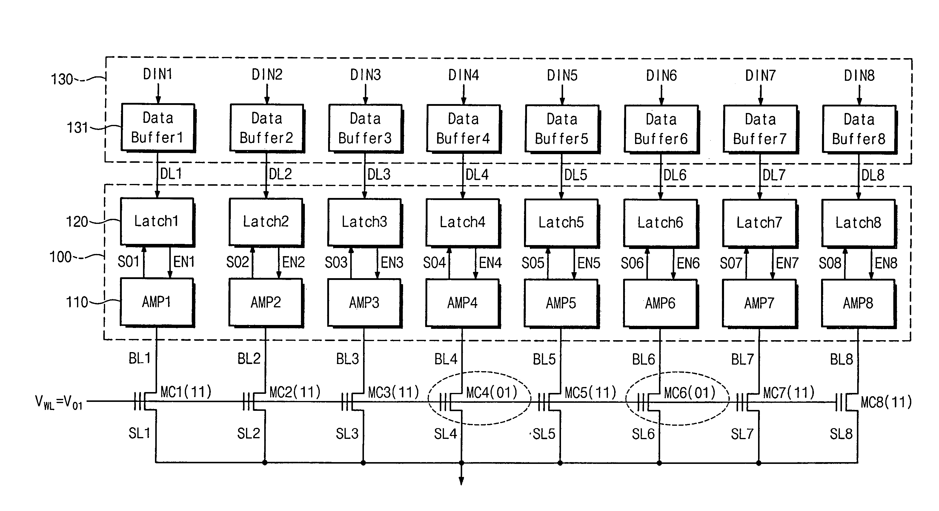
[0030]Exemplary embodiments of the invention are described below with reference to the corresponding drawings. These embodiments are presented as teaching examples. The actual scope of the invention is defined by the claims that follow.

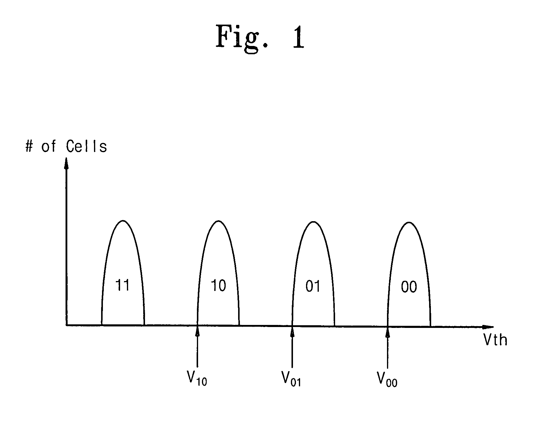
[0031]FIG. 1 is a graph showing a distribution profile for memory cell threshold voltages. An exemplary NOR flash memory device adapted to store multi_bit data is assumed for purposes of this explanation. Various program states for the exemplary NOR flash memory device correspond to the distribution of threshold voltages shown in FIG. 1.

[0032]Referring to FIG. 1, a memory cell may be placed into one of four states: “11”, “10”, “01”, and “00” using an appropriate threshold voltage. The “11” state in the illustrated example corresponds to an erased memory cell and has the lowest threshold voltage. The “10” state requires a higher threshold voltage than the “11” state. Similarly, the “01” state requires a higher threshold voltage than the “10” state, and...


PUM


Abstract

A NOR flash memory device and related programming method are disclosed. The programming method includes programming data in a memory cell and, during a program verification operation, controlling the supply of current from a sense amplifier to the memory cell in relation to the value of the programmed data. Wherein a program verification operation is indicated, current is provided from the sense amplifier to the memory cell. Where a program verification operation is not indicated, current is cut off from the sense amplifier.

Description

BACKGROUND OF THE INVENTION[0001]1. Field of the Invention[0002]Embodiments of the invention relate generally to semiconductor memory devices. More particularly, embodiments of the invention relate to NOR flash memory devices and programming methods for such devices.[0003]A claim of priority is made to Korean Patent Application No. 2005-68561 filed on Jul. 27, 2005, the subject matter of which is hereby incorporated by reference in its entirety.[0004]2. Description of Related Art[0005]Semiconductor memory devices generally store and read data, and may be classified as random access memories (RAMs) and read only memories (ROMs). RAMs are volatile memory devices that lose their stored data when power is interrupted. ROMs are non-volatile memory devices that continuously hold stored data even when power is interrupted. RAMs include dynamic RAM (DRAM) and static RAM (SRAM). ROMs include programmable ROM (PROM), erasable PROM (EPROM), electrically EPROM (EEPROM), and flash memory.[0006]F...

Claims


Application Information

Patent Timeline
Patent Type & Authority Patents(United States)
IPC IPC(8): G11C11/34G11C16/06
CPCG11C16/3454G11C16/12G11C16/10G11C16/34
Inventor KIM, BO-GEUNLIM, HEUNG-SOOIM, JAE-WOO
Owner SAMSUNG ELECTRONICS CO LTD
Why Eureka
Try Eureka