Semiconductor device

a semiconductor and memory device technology, applied in semiconductor devices, digital storage, instruments, etc., can solve the problems of increasing the number of manufacturing steps, complicated manufacturing process, and difficult for transistors of different conductivity types to have uniform transistor characteristics, so as to reduce the number of lines included in a cell array, the effect of preventing the leakage of charge from the capacitor

Active Publication Date: 2014-08-05
SEMICON ENERGY LAB CO LTD
View PDF125 Cites 14 Cited by
  • Summary
  • Abstract
  • Description
  • Claims
  • Application Information

AI Technical Summary

Benefits of technology

[0009]In view of the above problems, an object of the present invention is to propose a memory device in which memory capacity per unit area can be increased without making a manufacturing process complicated. Further, an object of the present invention is to propose a semiconductor device including a memory device, which is miniaturized and highly sophisticated by increasing memory capacity per unit area of the memory device without making a manufacturing process complicated while cost is reduced.
[0010]Each memory cell included in a DRAM is connected to a word line through which a signal for controlling switching of a switching element is supplied to the memory cell, a bit line for writing data to the memory cell and reading data from the memory cell, and a capacitor line for supplying a common potential which is connected to one electrode of a pair of electrodes of a capacitor. The present inventor has thought that the word line serves as the capacitor line, whereby the number of lines included in a cell array can be reduced.
[0013]In the memory device according to one embodiment of the present invention, a channel formation region of the transistor used as the switching element may include a semiconductor whose band gap is wider than that of silicon and whose intrinsic carrier density is lower than that of silicon. As such a semiconductor, for example, an oxide semiconductor, silicon carbide, gallium nitride, or the like which has approximately twice or more as wide band gap as silicon can be given. A transistor including the semiconductor can have much lower off-state current than a transistor including a normal semiconductor material such as silicon or germanium. The transistor having the above structure is used as a switching element for holding charge flowing into a capacitor, whereby leakage of charge from the capacitor can be prevented.
[0014]In the memory device according to one embodiment of the present invention, the word line serves as the capacitor line, whereby the number of lines included in a cell array can be reduced. Thus, the conductivity type of the transistors between the memory cells is not needed to be varied. Therefore, a memory device in which memory capacity per unit area is increased can be manufactured without making the manufacturing process complicated.
[0015]Further, in one embodiment of the present invention, a semiconductor device including a memory device, which is miniaturized and highly sophisticated by increasing memory capacity per unit area of the memory device without making a manufacturing process complicated while cost is reduced can be formed.

Problems solved by technology

The DRAM described in Patent Document 1 needs to use transistors of different conductivity types and thus has disadvantage of increasing the number of manufacturing steps as compared to a DRAM using a transistor of one conductivity type.
In addition, it is difficult for transistors of different conductivity types to have uniform transistor characteristics, such as an on-state current or a threshold voltage.
In order to have uniform transistor characteristics, process conditions, a transistor layout, and the like need to be controlled exactly, so that a manufacturing process becomes complicated.

Method used


Image

  • Semiconductor device
  • Semiconductor device
  • Semiconductor device

Examples


embodiment 1

(Embodiment 1)

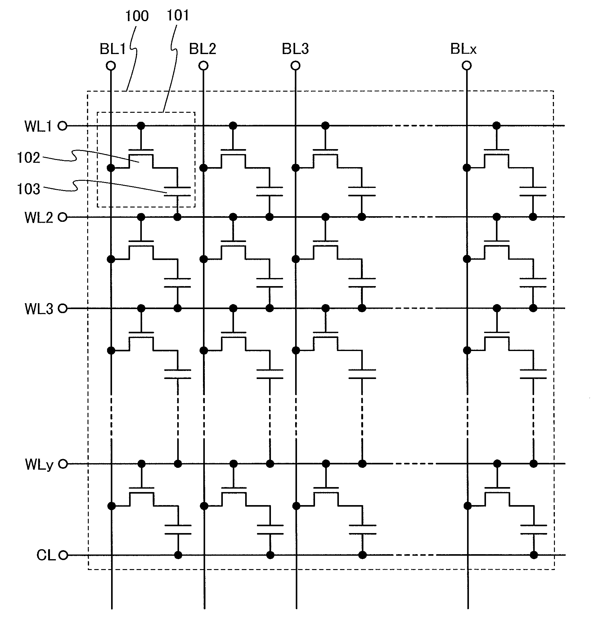
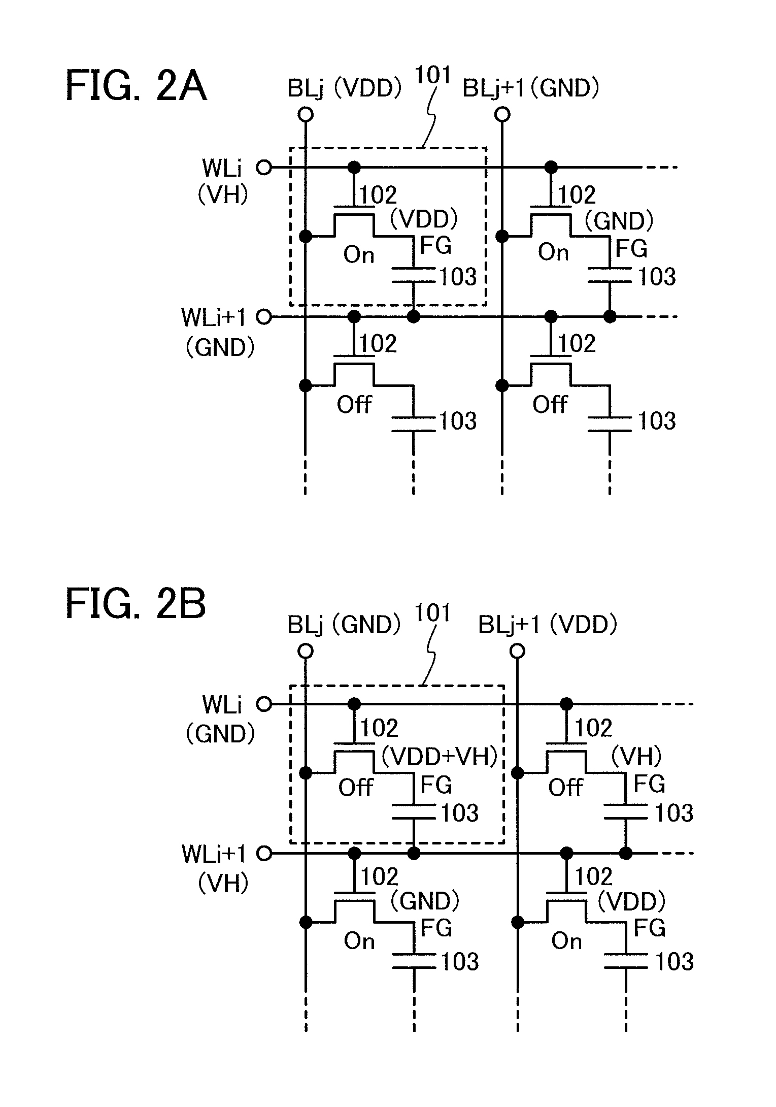
[0050]FIG. 1 shows an example of a circuit diagram of a structure of a cell array 100 in the memory device according to one embodiment of the present invention. The cell array 100 shown in FIG. 1 includes a plurality of memory cells 101 arranged in matrix, a plurality of word lines WL, and a plurality of bit lines BL. A signal from a driver circuit is supplied to each memory cell 101 through the plurality of word lines WL and the plurality of bit lines BL.

[0051]The number of the word lines WL and the number of the bit lines BL can be determined in accordance with the number of the memory cells 101 and arrangement of the memory cells 101. The cell array 100 shown in FIG. 1 includes memory cells 101 in x rows and y column (x and y are both natural numbers), word lines WL1 to WLy, and bit lines BL1 to BLx.

[0052]Each memory cell 101 includes a transistor 102 serving as a switching element and a capacitor 103. Note that the memory cell 101 may further include another circui...

embodiment 2

(Embodiment 2)

[0163]In this embodiment, a structure of a cell array 200 which is different from that of FIG. 1 in the memory device according to one embodiment of the present invention will be described.

[0164]FIG. 9 is an example of a circuit diagram showing a structure of the cell array 200 of this embodiment. In the cell array 200 shown in FIG. 9, a plurality of memory cells 201 is divided into two blocks: a first block 290 and a second block 291. The memory cell 201 included in the second block 291 is provided over a memory cell 201 included in the first block 290. That is, the cell array 200 in this embodiment has a structure in which the memory cells 201 are stacked.

[0165]Note that FIG. 9 shows an example in which the plurality of memory cells 201 is divided into two blocks: the first block 290 and the second block 291; however, the present invention is not limited to this structure. The memory device according to one embodiment of the present invention may have a structure in ...

embodiment 3

(Embodiment 3)

[0199]In this embodiment, a manufacturing method of a transistor forming a cell array will be described. Note that in this embodiment, a transistor formed using an oxide semiconductor will be described as an example.

[0200]First, as illustrated in FIG. 12A, an insulating film 701 is formed over a substrate 700, and conductive films 702 and conductive films 703 are formed over the insulating film 701. The conductive film 702 serves as a gate electrode of each of a transistor 712 and a transistor 713, and further serves as a word line. The conductive film 703 serves as another word line.

[0201]Although there is no particular limitation on a material which can be used as the substrate 700, it is necessary that the material have at least heat resistance high enough to withstand heat treatment to be performed later. For example, a glass substrate manufactured by a fusion process or a float process, a quartz substrate, a semiconductor substrate, a ceramic substrate, or the lik...


PUM


Abstract

Provided is a memory device in which memory capacity per unit area is increased without making the manufacturing process complicated. The memory device includes a plurality of memory cells, a plurality of word lines, and a plurality of bit lines. Each of the plurality of memory cells includes a switching element and a capacitor including a first electrode and a second electrode. In at least one of the plurality of memory cells, in accordance with a potential applied to one of the plurality of word lines, the switching element controls a connection between one of the plurality of bit lines and the first electrode, and the second electrode is connected to another one of the plurality of word lines.

Description

BACKGROUND OF THE INVENTION[0001]1. Field of the Invention[0002]The present invention relates to a memory device and a semiconductor device including the memory device.[0003]2. Description of the Related Art[0004]A DRAM (Dynamic Random Access Memory), which is one of semiconductor memory devices (hereinafter, also referred to just as memory devices), has a simple structure in which a memory cell includes a transistor and a capacitor (hereinafter, also referred to as a capacitor element). Thus, a DRAM needs fewer semiconductor elements for forming a memory cell than other memory devices such as an SRAM (Static Random Access Memory); therefore, memory capacity per unit area can be increased and cost can be reduced as compared to other memory devices.[0005]A DRAM is advantageous for large storage capacity as compared to other memory devices; however, memory capacity per unit area needs to be further increased as in other memory devices in order that an LSI having higher degree of integ...

Claims


Application Information

Patent Timeline
Patent Type & Authority Patents(United States)
IPC IPC(8): G11C11/24
CPCG11C11/401G11C5/02G11C5/063G11C8/14H01L29/7869H01L29/78696H01L29/78645H10B12/30
Inventor SAITO, TOSHIHIKO
Owner SEMICON ENERGY LAB CO LTD
Why Eureka
Try Eureka