LED package structure

a technology of led packaging and led chips, applied in the field of led package structures, can solve the problems of increasing the power consumption of the light chip, driving the luminance of the light chip to decrease, and unable to drive the luminance of the light chip to increase, so as to achieve the effect of improving the package structur

Active Publication Date: 2014-08-12
NAT CENT UNIV
View PDF1 Cites 1 Cited by
  • Summary
  • Abstract
  • Description
  • Claims
  • Application Information

AI Technical Summary

Benefits of technology

[0007]The main objective of the present inventi

Problems solved by technology

However, when the ambient environment is bright, the conventional LED device cannot drive the luminance of the light chip to decrease; when the ambient environment is dark, the conven

Method used


Image

  • LED package structure
  • LED package structure
  • LED package structure

Examples


first embodiment

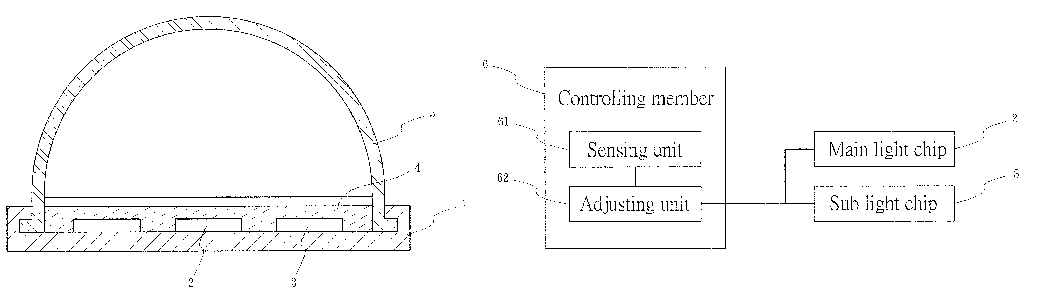
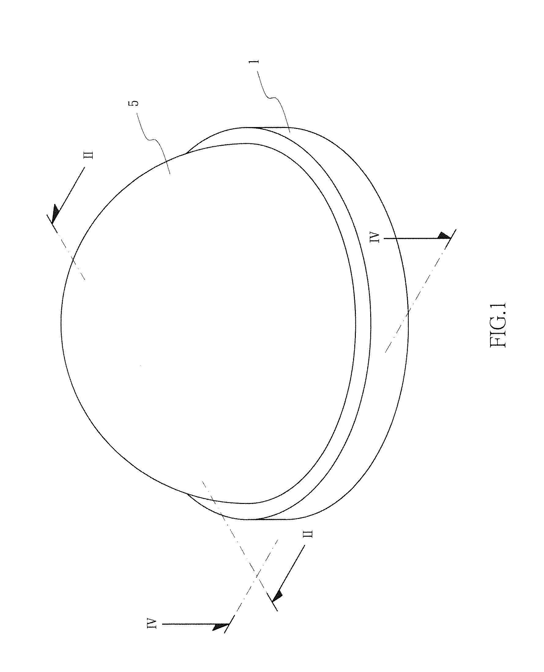
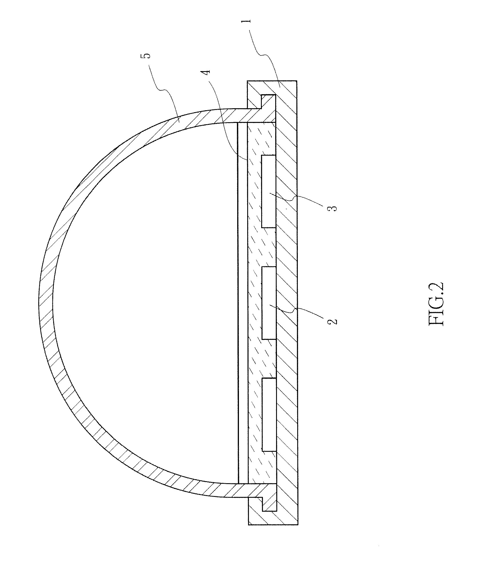
[0017]Referring to FIGS. 4-5, a first embodiment is described as following. The wavelength of each light beam from each main light chip 2 is 350 nm to 470 nm. The wavelength of each light beam from each sub light chip 3 is 480 nm to 570 nm. Each main light chip 2 is a blue LED. Each sub light chip 3 is a green LED. One main light chip 2 is positioned at a central portion of the base 1; four sub light chips 3 are positioned around the main light chip 2. The main light chip 2 and the sub light chips 3 are spaced from each other (the number of the main light chips 2 or the sub light chips 3 is not limited by the present invention.). Under this arrangement, when the ambient environment is bright, the controlling member 6 drives the luminance of each main light chip 2 to be higher than that of each sub light chip 3; when the ambient environment is dark, the controlling member 6 drives the luminance of each sub light chip 3 to be higher than that of each main light chip 2. Therefore, the ...

second embodiment

[0018]Referring to FIG. 6, a second embodiment is described as following. The wavelength of each light beam from each main light chip 2 is 350 nm to 470 nm. The wavelength of each light beam from each sub light chip 3 is 600 nm to 870 nm. Each main light chip 2 is a blue LED. Each sub light chip 3 is a red LED. The light beams from each main light chip 2 are mixed with the light beams from each sub light chip 3; in addition, a color rendition index of each mixed light beam is higher than that of each original light beam form each main light chip 2 or each sub light chip 3.

[0019]Referring to FIG. 3, the controlling member 6 has a sensing unit 61 and an adjusting unit 62. The adjusting unit 62 is electrically connected to the sensing unit 61. The adjusting unit 62 is electrically connected to each main light chip 2 and each sub light chip 3. Under this arrangement, the sensing unit 61 senses that the ambient environment is bright or dark; thereafter, the sensing unit 61 sends a signal...


PUM


Abstract

A LED package structure includes a base; at least one main light chip assembled to the base; a plurality of sub light chips assembled to the base; a wavelength shifter assembled to the base, the wavelength shifter located above each main light chip and each sub light chip, the wavelength shifter configured to shift a wavelength of each light beam from each main light chip; an outer lens assembled to the base and located above the wavelength shifter, so as to package each main light chip, each sub light chip and the wavelength shifter, the outer lens improving a light extraction efficiency of the light beams; and a controlling member electrically connected to each main light chip and each sub light chip, the controlling member configured to control luminance of each main light chip and luminance of each sub light chip.

Description

BACKGROUND OF THE INVENTION[0001]1. Field of the Invention[0002]The present invention relates to a package structure, and more particularly to a LED package structure.[0003]2. Description of Related Art[0004]A conventional LED device comprises a base; a light chip electrically assembled to the base; an outer lens assembled to the base and located above the light chip, so as to package the light chip.[0005]However, when the ambient environment is bright, the conventional LED device cannot drive the luminance of the light chip to decrease; when the ambient environment is dark, the conventional LED device cannot drive the luminance of the light chip to increase. Therefore, when the ambient environment is bright, a power consumption of the light chip cannot be decreased.[0006]The present invention has arisen to mitigate and / or obviate the disadvantages of the conventional.SUMMARY OF THE INVENTION[0007]The main objective of the present invention is to provide an improved package structur...

Claims


Application Information

Patent Timeline
IPC IPC(8): H05B37/02F21V7/00
CPCF21V7/00H05B37/02F21V23/0464F21Y2113/007F21Y2101/02H05B33/0821F21Y2113/17F21Y2115/10H05B45/40
Inventor SUN, CHING-CHERNGCHANG, YU-YUCHEN, CHING-YI
Owner NAT CENT UNIV
Why Eureka
Try Eureka