Integrated circuit and method for testing memory on the integrated circuit

a technology of integrated circuits and integrated circuits, applied in the direction of electronic circuit testing, static storage, measurement devices, etc., can solve the problems of bringing its own testing problems, externally generated test vector style tests are not suitable for verifying embedded memory arrays, and the time spent in manufacturing tests is exponentially increased

Active Publication Date: 2014-09-16
ARM LTD
View PDF58 Cites 12 Cited by
  • Summary
  • Abstract
  • Description
  • Claims
  • Application Information

AI Technical Summary

Benefits of technology

[0022]Such an approach hence provides a very simple programmer's view of the memory test system, allowing any transactions to be targeted at any individual memory unit, or at arbitrary combinations of memory units as defined by the memory groups. This hence avoids the problem with typical prior art techniques that results in a complex programmer's model based around variable length shift registers, the order of memory components in the scan chain, and many other factors.
[0029]In one embodiment, at least one of the groups of memory units is programmable. This provides significant flexibility when performing testing. For example, if as a result of testing performed on particular predefined groups, it can be determined that a test fail condition is due to a failure in a memory unit in one particular predefined group, then the programmable group can be programmed to identify a predetermined subset of the memory units in that problematic predefined group with the aim of seeking to locate the exact memory unit giving rise to the error.
[0037]In one embodiment employing a ring bus, each memory test module employs a handshaking protocol to control propagation of the transaction around the ring bus. The handshaking protocol can take a variety of forms, for example a valid / ready protocol where a transmitting device issuing data (e.g. a transaction) asserts a valid signal with that data, and maintains the data until an asserted ready signal is received from the recipient indicating that the recipient was able to receive that data. By using such a handshaking protocol, it is possible to accelerate the onward propagation of the transaction, or at least part of the transaction, through the series of memory test modules. For example, if a transaction passing around the ring bus is seeking to read a particular status register, and within a particular memory test module a test is still in the process of being performed such that the status register is not yet available to be read, then the first and second address portions of that transaction can still be forwarded on by that memory test module to the next memory test module in the series even if the associated data portion cannot yet be transmitted. In that instance, the memory test module in question will de-assert its valid signal once the first and second address portions have been successfully transmitted onto the next memory test module in the series, and will not assert its valid signal again until the data portion is ready to transmit. Similarly, that memory test module could de-assert its ready signal if, due to the time taken to perform the test operation within the memory test module, it is unable to receive a next transaction seeking to be passed to it from a memory test module upstream of it.

Problems solved by technology

Whilst embedded memory presents significant system performance and cost reduction advantages, it brings its own testing issues.
Externally generated test vector style tests are not suitable for verifying embedded memory arrays for a number of reasons.
Firstly, the time spent in the manufacturing test grows exponentially as the embedded memory die area increases, which often makes such test vector style testing too costly.
However, as the number of memory circuits provided within the integrated circuit increases, such an approach results in the chip area devoted to testing becoming unacceptably large.
March tests (or test algorithms) are applied one memory operation at a time, and as a result multiple operations cannot be applied at system clock speed.
As the number of memory units embedded within the integrated circuit increases, then this results in an increase in the complexity of the interface between those memory units and a shared BIST mechanism for those memory units.
The known BIST mechanism sharing techniques become complex to manage as the number of memory units increase, and further lack flexibility with regard to the tests to be applied on each of the memory units.

Method used


Image

  • Integrated circuit and method for testing memory on the integrated circuit
  • Integrated circuit and method for testing memory on the integrated circuit
  • Integrated circuit and method for testing memory on the integrated circuit

Examples


Embodiment Construction

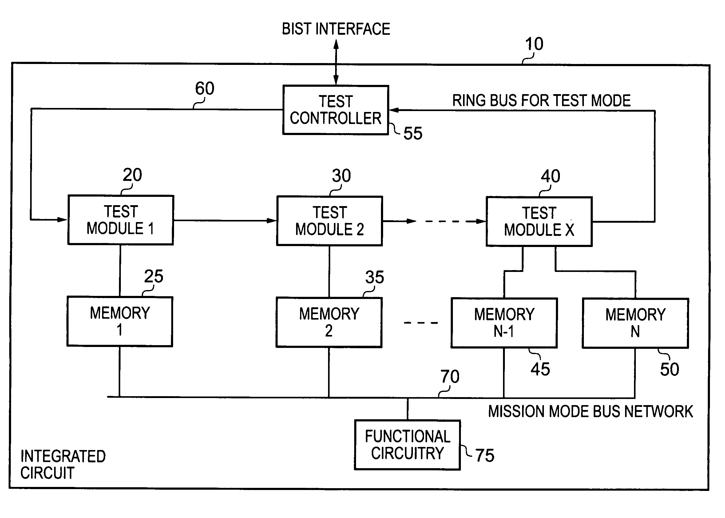
[0061]FIG. 1 is a block diagram of an integrated circuit in accordance with one embodiment. The integrated circuit 10 comprises a plurality of embedded memory units 25, 35, 45, 50 which are used by a number of functional circuits (denoted in FIG. 1 as functional circuitry 75) during a normal mode of operation (also referred to herein as a mission mode). During the mission mode, the various functional circuits 75 will access the associated memory units 25, 35, 45, 50 via a bus network 70. The bus network can take a variety of forms as will be understood by those skilled in the art, but will allow each of the memory units to be accessed by one or more functional circuits during the mission mode of operation to enable read and / or write operations to take place in respect of those memory units.

[0062]As also shown in FIG. 1, a plurality of test modules 20, 30, 40 are provided for use during a test mode of operation to perform test operations in respect of the various memory units 25, 35,...


PUM


Abstract

An integrated circuit includes memory units and at least one memory test module, each module includes one associated memory unit, a set of test registers therefor, and a test engine configured to perform a test operation on that associated memory unit. A transaction interface of the memory test module receives a transaction specifying a register access operation and providing a first address portion having encodings allowing individual memory units as well as groups of memory units to be identified, and a second address portion identifying one of the test registers within the set to be an accessed register. Decode circuitry, within each memory test module and responsive to the transaction, is configured to selectively perform the register access operation if it is determined that the memory test module includes a set of test registers associated with a memory unit.

Description

BACKGROUND OF THE INVENTION[0001]1. Field of the Invention[0002]The present invention relates to an integrated circuit and method for testing memory on the integrated circuit.[0003]2. Description of the Prior Art[0004]It is becoming more and more common for integrated circuits to include embedded memory to allow rapid access to data by functional circuits provided on the integrated circuit. Whilst an integrated circuit may traditionally comprise a number of circuit components formed on a single die, it may also consist of circuit components distributed across multiple dies that are integrated together in a package using 3D integration technologies such as multi-chip modules, system in package, or through-silicon-vias.[0005]As the use of embedded memory continues to increase, thorough testing and defect diagnosis has become a key requirement to ensure product quality and enhance product yield. Whilst embedded memory presents significant system performance and cost reduction advantage...

Claims


Application Information

Patent Timeline
Patent Type & Authority Patents(United States)
IPC IPC(8): G11C29/00G01R31/28G11C29/04G11C29/16G11C29/26
CPCG11C29/16G11C2029/0401G11C2029/2602
Inventor HUGHES, PAUL, STANLEY
Owner ARM LTD
Why Eureka
Try Eureka