Shift register

a technology of shift register and shift node, which is applied in the field of shift register, can solve the problems of high leakage of charges at the set node of a stage, and the normal output of scan pulses, so as to prevent the leakage of charges

Active Publication Date: 2014-09-23
LG DISPLAY CO LTD
View PDF10 Cites 6 Cited by
  • Summary
  • Abstract
  • Description
  • Claims
  • Application Information

AI Technical Summary

Benefits of technology

[0008]An object of the present invention is to provide a shift register which generates a carry pulse using a carry clock pulse, which is kept high for a longer time than a scan clock pulse, and turns on a specific switching device for a sufficient time including a low duration between scan pulses using the carry pulse, so as to prevent leakage of charges at a set node.

Problems solved by technology

As a result, in this low duration, the possibility that charges at a set node of a stage will be leaked is higher.
For this reason, there may occur a problem that the scan pulse is not normally output in an output period of the stage.

Method used


Image

  • Shift register
  • Shift register
  • Shift register

Examples


first embodiment

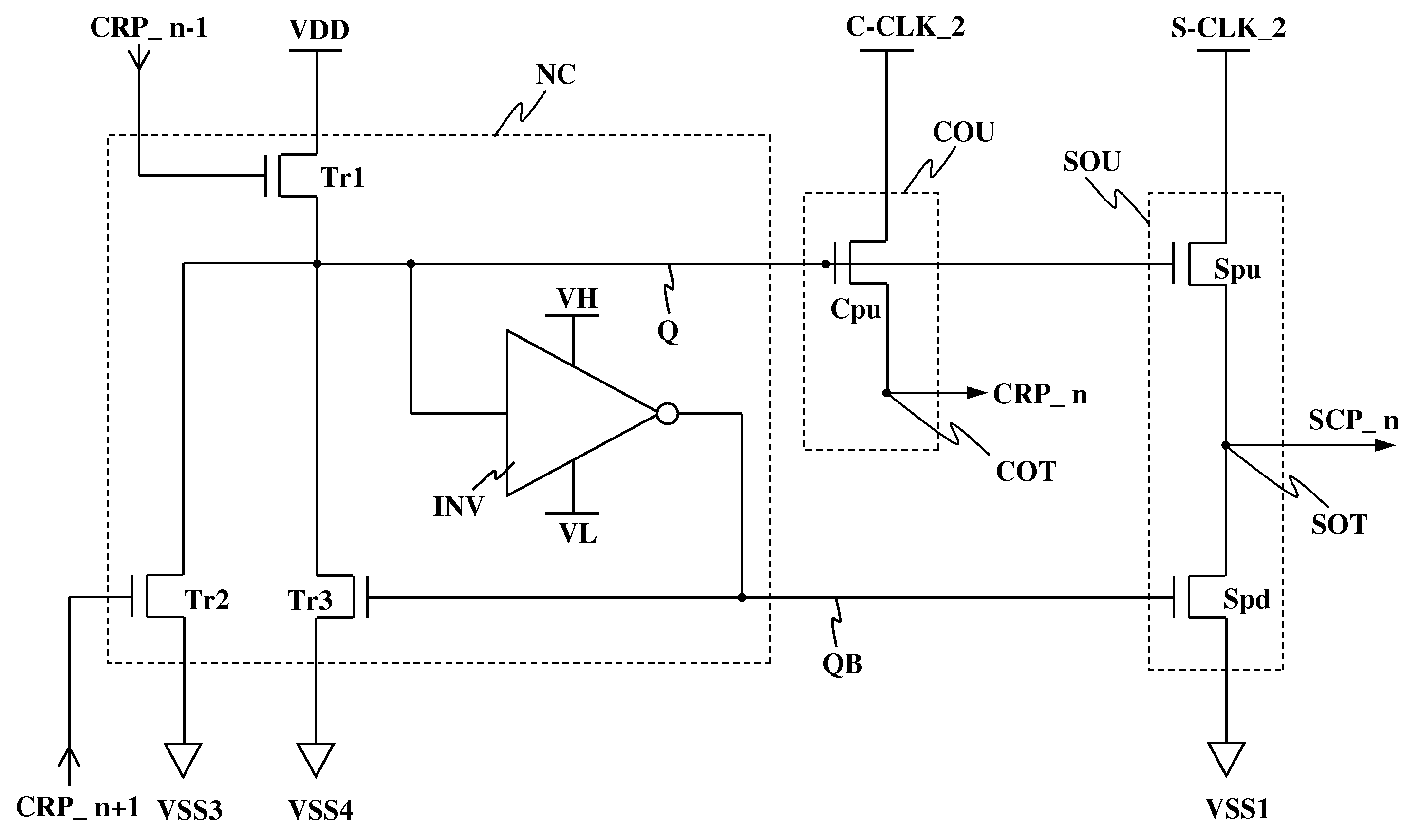
[0080]FIG. 4 is a circuit diagram of an arbitrary stage in FIG. 3.

[0081]The arbitrary stage, for example, the nth stage ST_n includes a set node Q, a reset node QB, a carry output terminal COT, a scan output terminal SOT, a node controller NC, a carry output unit COU, and a scan output unit SOU, as shown in FIG. 4.

[0082]The node controller NC of the nth stage ST_n controls voltages at the set node Q and reset node QB in response to a carry pulse CRP_n−1 from an upstream stage and a carry pulse CRP_n+1 from a downstream stage. To this end, the node controller NC of the nth stage ST_n includes first to third switching devices Tr1 to Tr3 and an inverter INV, as shown in FIG. 4.

[0083]The carry output unit COU of the nth stage ST_n includes a carry pull-up switching device Cpu, as shown in FIG. 4.

[0084]The scan output unit SOU of the nth stage ST_n includes a scan pull-up switching device Spu and a scan pull-down switching device Spd, as shown in FIG. 4.

[0085]Hereinafter, a detailed desc...

second embodiment

[0098]FIG. 5B is a circuit diagram of the inverter INV in FIG. 4.

[0099]The inverter INV of the arbitrary stage, for example, the nth stage ST_n may include first to third inverting switching devices iTr1 to iTr3, as shown in FIG. 5B.

[0100]The first inverting switching device iTr1 of the nth stage ST_n is controlled by an external control signal CS and is connected between a high voltage line and the reset node QB. That is, the first inverting switching device iTr1 is turned on or off in response to the control signal CS, and interconnects the high voltage line and the reset node QB when turned on.

[0101]The second and third inverting switching devices iTr2 and iTr3 of the nth stage ST_n are the same in configuration as the above-stated second and third inverting switching devices iTr2 and iTr3 in FIG. 5A, respectively, and a functional description thereof will thus be replaced by the above description given with reference to FIG. 5A.

third embodiment

[0102]FIG. 5C is a circuit diagram of the inverter INV in FIG. 4.

[0103]The inverter INV of the arbitrary stage, for example, the nth stage ST_n may include first to fifth inverting switching devices iTr1 to iTr5, as shown in FIG. 5C.

[0104]The first inverting switching device iTr1 of the nth stage ST_n is controlled by a high voltage VH from a high voltage line and is connected between the high voltage line and a common node CN. That is, the first inverting switching device iTr1 is turned on or off in response to the high voltage VH, and interconnects the high voltage line and the common node CN when turned on.

[0105]The second inverting switching device iTr2 of the nth stage ST_n is controlled by the voltage at the set node Q and is connected between the common node CN and a low voltage line. That is, the second inverting switching device iTr2 is turned on or off in response to the voltage at the set node Q, and interconnects the common node CN and the low voltage line when turned on...


PUM


Abstract

Disclosed herein is a shift register which is capable of preventing leakage of charges at a set node which occurs when the duty ratio of a scan pulse is small, so as to normally output a scan pulse. The shift register includes a plurality of stages for sequentially generating outputs thereof. Each of the stages includes a carry output unit for outputting a carry pulse to drive at least one of a downstream stage and an upstream stage, and a scan output unit for outputting a scan pulse to drive a gate line. Each of the outputs generated from the stages includes the carry pulse and the scan pulse. The carry pulse and the scan pulse are paired to correspond to each other. The paired carry pulse and scan pulse have different durations.

Description

[0001]This application claims the benefit of Korean Patent Application No. 10-2012-0086575, filed on Aug. 8, 2012, which is hereby incorporated by reference as if fully set forth herein.BACKGROUND OF THE INVENTION[0002]1. Field of the Invention[0003]The present invention relates to a shift register, and more particularly, to a shift register which is capable of preventing leakage of charges at a set node which occurs when the duty ratio of a scan pulse is small, so as to normally output a scan pulse.[0004]2. Discussion of the Related Art[0005]A shift register outputs a plurality of scan pulses in order to sequentially drive gate lines of a display device, such as a liquid crystal display.[0006]A scan pulse has a duty ratio that can be set appropriately according to a given driving condition. In particular, when the duty ratio of the scan pulse is smaller, a duration in which the scan pulse is kept low (referred to hereinafter as a low duration) is longer. As a result, in this low du...

Claims


Application Information

Patent Timeline
Patent Type & Authority Patents(United States)
IPC IPC(8): G09G3/36G09G3/20G11C19/00G11C19/28
CPCG11C19/287G11C19/28G09G2310/0291G09G3/3677G09G3/36G09G3/20G09G2310/0267G11C19/00
Inventor JANG, YONG-HO
Owner LG DISPLAY CO LTD
Why Eureka
Try Eureka