Test system of reconfigurable device and its method and reconfigurable device for use therein

a reconfigurable device and test system technology, applied in the direction of electronic circuit testing, measurement devices, instruments, etc., can solve the problem of long test time, reduce the number of times data is loaded, and reduce the time needed for tests

Inactive Publication Date: 2014-09-23
NEC CORP
View PDF18 Cites 33 Cited by
  • Summary
  • Abstract
  • Description
  • Claims
  • Application Information

AI Technical Summary

Benefits of technology

[0018]In such a conventional test scheme, test configuration data and transfer configuration data must be alternately and repeatedly loaded into the FPGA (steps 510 and 550), causing a problem in which the test time becomes long. In comparison with test input data comparable to a test vector of normal LSI, the FPGA involves more test and transfer configuration data which take longer to load. It is therefore desired to reduce the number of times the configuration data is loaded in order to reduce the test time.
[0032]Effects of the present invention will be described. A reconfigurable device used herein holds a plurality of configuration data and is capable of instantaneously switching which configuration is implemented thereby. Specifically, one transfer configuration data and one or more test configuration data are previously loaded in the reconfigurable device, and a test is made while sequentially switching the transfer configuration data and the test configuration data. In this way, the same configuration data need not be reloaded a number of times, so that the test can be made in which the number of times that the data is loaded is reduced compared with previously.
[0033]According to the present invention, one or more test configuration data and one transfer configuration data are loaded in a memory of a reconfigurable device such that tests are performed using them again and again as appropriate, so that the test can be made with the advantage that the number of times that the data is loaded is reduced which consequently reduces the time needed for the tests.

Problems solved by technology

In such a conventional test scheme, test configuration data and transfer configuration data must be alternately and repeatedly loaded into the FPGA (steps 510 and 550), causing a problem in which the test time becomes long.

Method used


Image

  • Test system of reconfigurable device and its method and reconfigurable device for use therein
  • Test system of reconfigurable device and its method and reconfigurable device for use therein
  • Test system of reconfigurable device and its method and reconfigurable device for use therein

Examples


first embodiment

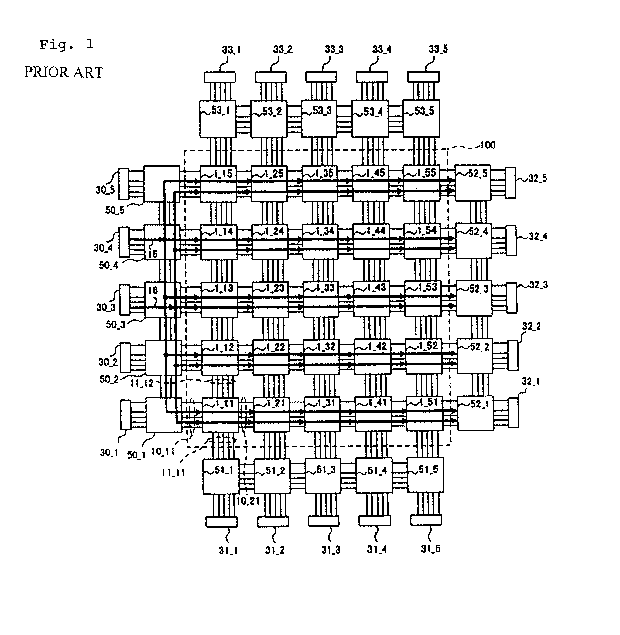
[0109]Next, a description will be given of a transfer configuration in the present invention with reference to FIG. 12. In FIG. 12, bold arrows represent signal path 18—y in the transfer configuration. In other words, logic blocks in each row are connected from left to right in series, and the output of each row is input to peripheral block 52—y. Here, y is an integer indicative of the coordinate of the block.

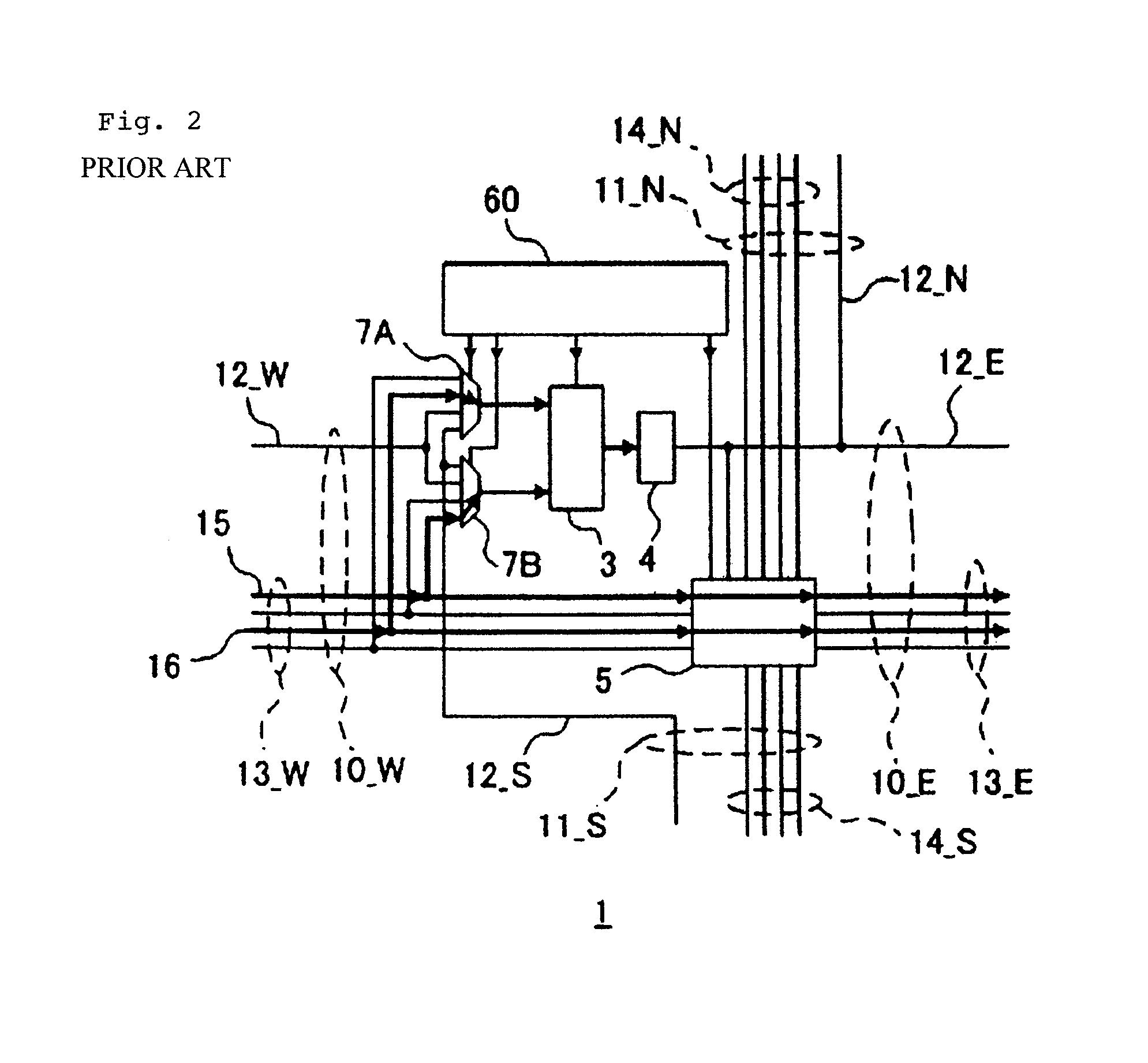
[0110]Signal paths within a logic block in the transfer configuration are shown in FIG. 13. Bold arrows in FIG. 13 represent signal paths within each logic block 1. Input selector 7A is configured to output a signal on programmable wire 12_W, while functional element 3 is configured to output the output of input selector 7A as it is. Output 12_E of register 4 is connected to programmable wire 12_W of a left-hand adjacent logic block.

[0111]In FIG. 12, in the transfer configuration, registers 4 in logic blocks of each row are sequentially connected from left to right in a one-to-...

fourth embodiment

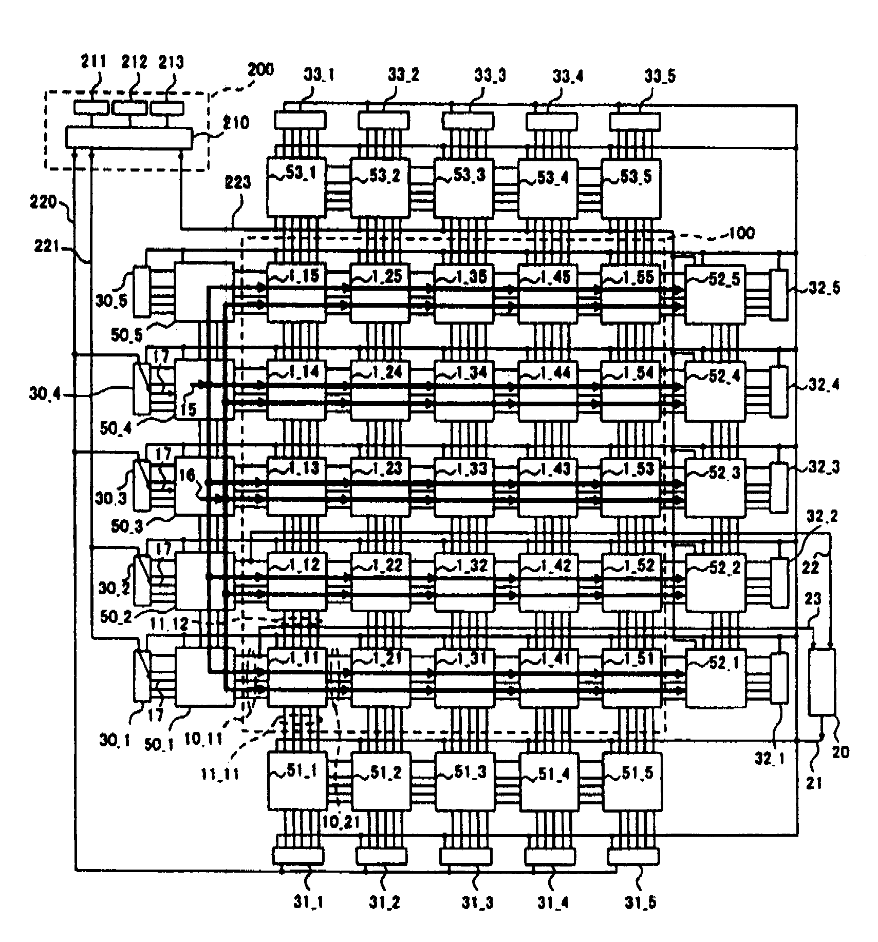
[0157]In the present invention, signals corresponding to outputs 220, 221, 223 from test controller 200 in FIG. 6 are distributed using programmable wires. In this way, a test only circuit need not be embedded in the device. Advantageously, since the test function is implemented by logic blocks, the test function can be modified after the device is manufactured. Also, the area can be saved because a test only circuit is not required.

[0158]It should be noted that a separate test is made for the logic blocks used to implement the test logic and comparator. Here, while a description has been given of an example in which all functions of the test controller and comparator are implemented by the logic blocks, those skilled in the art could readily contemplate an exemplary modification in which only part of these functions is implemented by logic blocks, while the rest is implemented by dedicated circuits.

[0159]While a description has been given of a reconfigurable device of a particular ...


PUM


Abstract

A reconfigurable device test scheme is provided for making a test of a reconfigurable device with configuration data which is loaded a smaller number of times. A reconfigurable device used herein holds a plurality of configuration data and is capable of instantaneously switching which configuration is implemented thereby. Specifically, one transfer configuration data and one or more test configuration data are previously loaded in a configuration memory of the reconfigurable device, and a test is made while sequentially switching the transfer configuration data and the test configuration data. In this way, the same configuration data need not be reloaded over and over, so that the test can be made with a smaller number of times of loading as compared with before.

Description

TECHNICAL FIELD[0001]The present invention relates to a system for and a method of testing a reconfigurable device, and a reconfigurable device for use therewith.BACKGROUND ART[0002]FIG. 1 shows exemplary blocks of an FPGA (Field Programmable Gate Array) which is a conventional reconfigurable device. The FPGA comprises logic block array 100, input / output blocks 30—y, 31—x, 32—y, 33—x responsible for data input / output outside the chip, peripheral blocks 50—y, 51—x, 52—y, 53—x which mediate both, and programmable wires (for example, 10_11, 10_21, 11_11, 11_12) for programmably connecting between these blocks. Logic block array 100 is a two-dimensional array of logic blocks 1_xy. Here, x, y are integers indicative of the position of each block.[0003]FIG. 1 illustrates logic block array 100 which is comprised of logic blocks in five rows and five columns (i.e., x and y are integers from one to five, respectively), but in general, the size of a logic block array in an FPGA may be arbitra...

Claims


Application Information

Patent Timeline
Patent Type & Authority Patents(United States)
IPC IPC(8): G01R31/28G01R31/3185
CPCG01R31/318516
Inventor NAKAYA, SHOGO
Owner NEC CORP
Why Eureka
Try Eureka