Memory device having stitched arrays of 4 F2 memory cells

a memory device and array technology, applied in the field of memory devices having stitched arrays of memory cells, can solve the problems of reducing the size of the memory cell, complicating the scaling of the device, and affecting the scaling of the conventional transistor, so as to minimize the layout complexity and space usage.

Active Publication Date: 2014-11-04
AVALANCHE TECH
View PDF24 Cites 5 Cited by
  • Summary
  • Abstract
  • Description
  • Claims
  • Application Information

AI Technical Summary

Benefits of technology

[0009]The present invention provides a stitching architecture for connecting local electrodes of memory arrays having 4 F2 memory cells to main device wiring lines while minimizing both layout complexity and space usage.

Problems solved by technology

While a memory device employing the selection transistor is more suitable for the random access type of memories, the more complicated structure of the selection transistor means the size of the memory cell will be larger, which translates to a lower cell density.
Moreover, the memory device utilizing the selection transistor needs additional wiring for controlling the gate electrode, further complicating the scaling of the device.
However, several difficulties can arise when scaling down a conventional transistor, particularly its channel length, to sizes of a few tens of nanometers.
As the channel length is reduced, there is a propensity for the formation of parasitic conduction paths between source and drain, thereby causing punch through current leakages.
Another obstacle encountered in shrinking the conventional transistor is reduced current drivability caused by the reduced width of the current carrying channel.
This is a significant issue for resistive memory devices, which require higher current to switch their memory state.

Method used


Image

  • Memory device having stitched arrays of 4 F2 memory cells
  • Memory device having stitched arrays of 4 F2 memory cells
  • Memory device having stitched arrays of 4 F2 memory cells

Examples


Embodiment Construction

[0023]The present invention provides memory devices having 4 F2 memory cells, including means for connecting arrays of memory cells to main wiring lines and to each other.

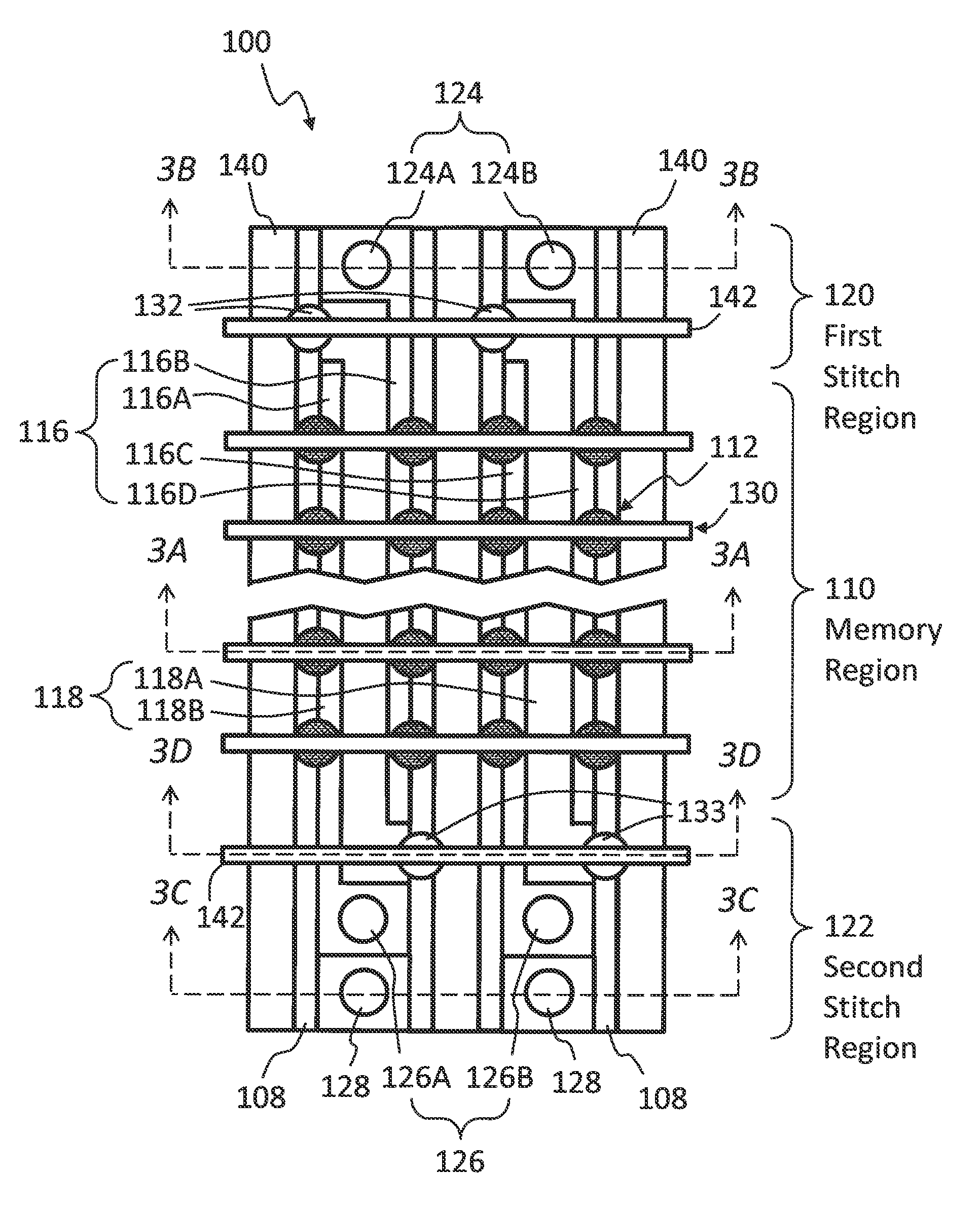
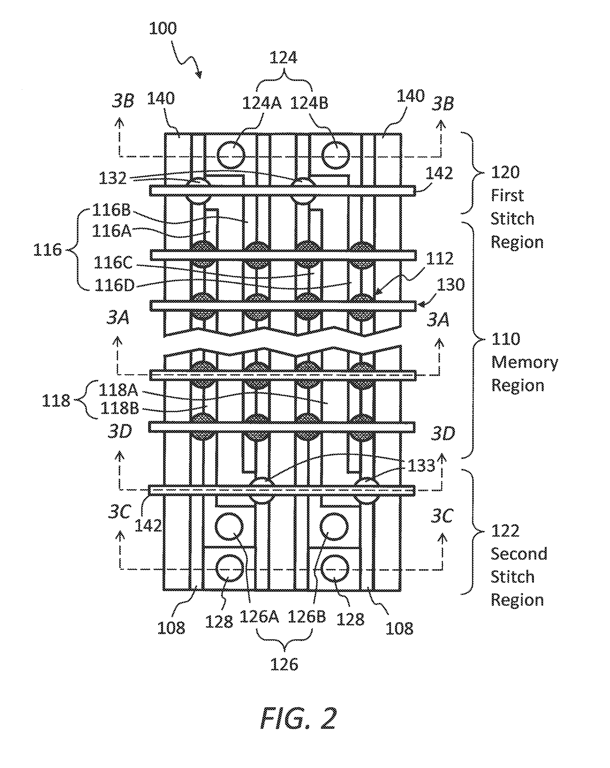
[0024]An embodiment of the present invention as applied to a memory device having an array of 4 F2 memory cells will now be described with reference to FIG. 2 and FIGS. 3A-3D. FIG. 2 is a top view and FIGS. 3A-3D are corresponding cross sectional views of a memory array 100. In these drawings the insulation material separating various elements is omitted for reasons of clarity. With continuing reference to FIG. 2 and FIGS. 3A-3D, the illustrated memory array 100 comprises a semiconductor substrate 102 having a plurality of parallel trenches 104 therein, each of the trenches having a respective one of a plurality of trench bottoms 106 and a respective pair of a plurality of paired trench sidewalls 108; a memory region 110 formed in the semiconductor substrate 102 including an array of memory cells 112 having a plura...


PUM


Abstract

A memory device comprises a semiconductor substrate having a plurality of parallel trenches therein, a memory region formed in the substrate including an array of memory cells having a plurality of vertical selection transistors with respective channels formed in trench sidewalls, a plurality of buried source electrodes in trench bottoms, a plurality of paired gate electrodes formed on paired trench sidewalls, a first and second stitch region disposed adjacent the memory region along a trench direction including a first and second row of gate contacts, respectively, and a row of source contacts disposed in the first or second stitch region with each of the source contacts coupled to a respective one of the source electrodes. One of each pair of the gate electrodes is coupled to a respective one of the first row of gate contacts and the other one of each pair of gate electrodes is coupled to a respective one of the second row of gate contacts.

Description

RELATED APPLICATIONS[0001]The present application is related to U.S. provisional patent application Ser. No. 61 / 562,309, filed Nov. 21, 2011, for MEMORY DEVICE INCLUDING TRANSISTOR ARRAY SHARING COMMON CHANNEL AND PROCESS FOR MAKING THE SAME, by SATOH et al., included by reference herein and for which benefit of the priority date is hereby claimed.FIELD OF THE INVENTION[0002]The present invention relates to semiconductor memory architectures, particularly to memory devices having stitched arrays of memory cells.BACKGROUND OF THE INVENTION[0003]Resistive memory is a new class of non-volatile memory, which can retain the stored information when powered off. A resistive memory device normally comprises an array of memory cells, each of which includes at least a resistive memory element and a selection element coupled in series between appropriate electrodes. Upon application of an appropriate voltage or current to the resistive memory element, the electrical resistance of the resistive...

Claims


Application Information

Patent Timeline
Patent Type & Authority Patents(United States)
IPC IPC(8): H01L29/04H01L45/00H01L29/78H01L27/115
CPCH01L45/145H01L29/7827H01L45/144H01L45/04H01L27/11514H01L27/2454H01L45/06H01L45/08H01L45/1233H01L27/2463H01L27/11507H01L45/085H01L27/2481H01L27/228H01L27/2436H01L43/02H01L43/08H01L45/146H01L45/147H10B63/34H10B61/22H10B63/80H10N70/245H10N70/8836H10N70/231H10N70/8828H10N70/8833H10N70/826H10B53/20H10B53/30H10B63/30H10B63/84H10N50/10H10N50/80H10N70/20H10N70/24H10N70/883
Inventor SATOH, KIMIHIROHUAI, YIMING
Owner AVALANCHE TECH
Why Eureka
Try Eureka