Optoelectronic semiconductor component

Active Publication Date: 2014-12-09
OSRAM OLED
View PDF11 Cites 1 Cited by
  • Summary
  • Abstract
  • Description
  • Claims
  • Application Information

AI Technical Summary

Benefits of technology

[0028]Alternatively, the connection layer can also comprise a transparent conductive oxide such as ITO, for example, wherein the connection layer is succeeded preferably by a mirror layer as seen from the active layer. In this case, the mirror layer can be a layer composed of a metal or a metal alloy. Particularly preferably, the mirror layer is a dielectric mirror in this configuration. The dielectric mirror advantageously comprises a multiplicity of alternating layers composed of two dielectric materials hav

Problems solved by technology

When a p-doped nitride compound semiconductor layer is connected to an electrical connection layer, undesirably high voltage drops often occur at the

Method used


Image

  • Optoelectronic semiconductor component
  • Optoelectronic semiconductor component
  • Optoelectronic semiconductor component

Examples


Example

DETAILED DESCRIPTION OF THE DRAWINGS

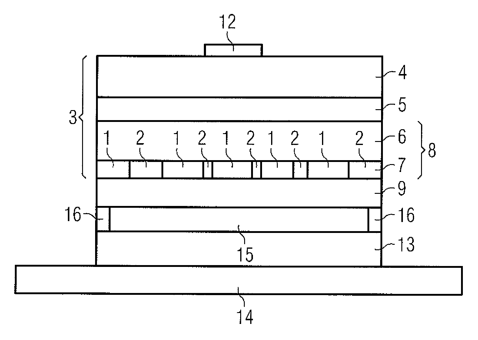
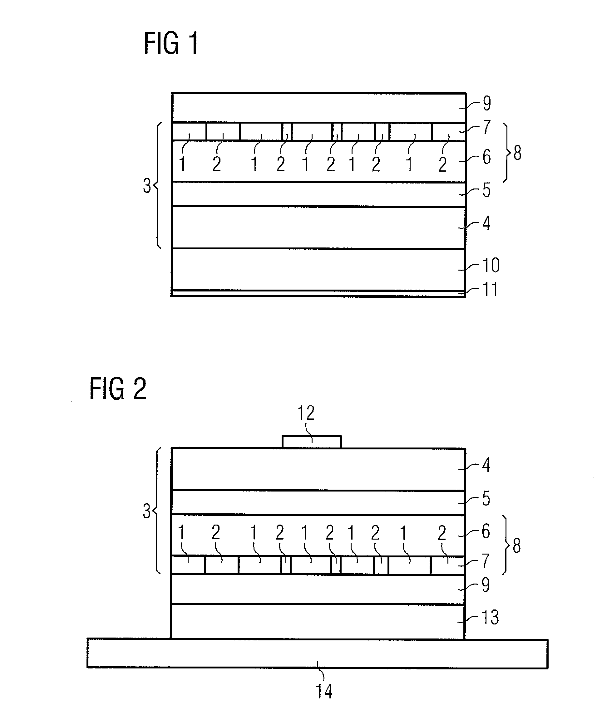
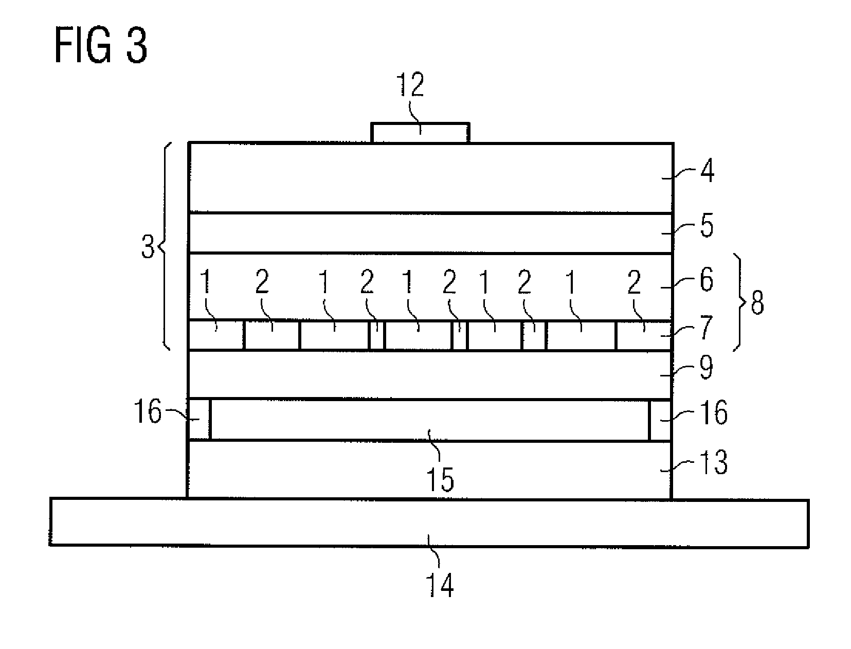
[0034]Identical or identically acting constituent parts are provided with the same reference symbols in each case in the figures. The constituent parts illustrated and also the size relationships of the constituent parts among one another should not be regarded as true to scale.

[0035]The optoelectronic semiconductor component illustrated in FIG. 1 contains a semiconductor layer sequence 3 based on a nitride compound semiconductor material.

[0036]The semiconductor layers 4, 5, 6, 7 of the semiconductor layer sequence 3 therefore comprise, in particular, InxAlyGa1-x-yN where 0≦x≦1, 0≦y≦1 and x+y≦1.

[0037]The semiconductor layer sequence 3 is grown for example epitaxially onto a growth substrate 10. The growth substrate 10 is, for example, a sapphire substrate or a GaN substrate.

[0038]The semiconductor layer sequence 3 contains an n-doped region 4, a p-doped region 8 and an active layer 5 arranged between the n-doped region 4 and the p-doped region 8.

[...


PUM


Abstract

An optoelectronic semiconductor component comprising a semiconductor layer sequence (3) based on a nitride compound semiconductor and containing an n-doped region (4), a p-doped region (8) and an active zone (5) arranged between the n-doped region (4) and the p-doped region (8) is specified. The p-doped region (8) comprises a p-type contact layer (7) composed of InxAlyGa1-x-yN where 0≦x≦1, 0≦y≦1 and x+y≦1. The p-type contact layer (7) adjoins a connection layer (9) composed of a metal, a metal alloy or a transparent conductive oxide, wherein the p-type contact layer (7) has first domains (1) having a Ga-face orientation and second domains (2) having an N-face orientation at an interface with the connection layer (9).

Description

RELATED APPLICATIONS[0001]This is a U.S. national stage of application No. PCT / DE2009 / 001322, filed on Sep. 16, 2009.[0002]This patent application claims the priority of German Patent Application No. 10 2008 052 405.0, filed Oct. 21, 2008, the disclosure content of which is hereby incorporated by reference.FIELD OF THE INVENTION[0003]The invention relates to an optoelectronic semiconductor component, in particular a component based on a nitride compound semiconductor, such as, for example, an LED or a laser diode.BACKGROUND OF THE INVENTION[0004]An optoelectronic semiconductor component generally comprises an n-doped region, a p-doped region and a radiation-emitting or radiation-receiving active zone arranged therebetween. In order to produce an electrical connection, the p-doped region and the n-doped region are provided with a connection layer at least in a partial region. The connection layer can be, for example, a metal layer or a layer composed of a transparent conductive oxide...

Claims


Application Information

Patent Timeline
IPC IPC(8): H01L33/40H01L33/60
CPCH01L33/40H01L2924/0002H01L2924/00
Inventor STRASSBURG, MARTINHOPPEL, LUTZPETER, MATTHIASZEHNDER, ULRICHTAKI, TETSUYALEBER, ANDREASBUTENDEICH, RAINERBAUER, THOMAS
Owner OSRAM OLED
Why Eureka
Try Eureka