Three-dimensional non-volatile memory device, memory system including the same and method of manufacturing the same

a memory device and non-volatile technology, applied in the field of semiconductor devices, can solve the problems of increasing the time taken for cells to be programmed, preventing higher levels of integration, etc., and achieve the effect of reducing capacitance between word lines and improving cell program speed

Active Publication Date: 2014-12-16
SK HYNIX INC
View PDF11 Cites 30 Cited by
  • Summary
  • Abstract
  • Description
  • Claims
  • Application Information

AI Technical Summary

Benefits of technology

[0010]An embodiment of the present invention relates to a three-dimensional non-volatile memory device configured to improve the program speed of cells by reducing capacitance between word lines and a method of manufacturing the same.

Problems solved by technology

Two-dimensional memory devices in which memory cells are fabricated in a single layer over a silicon substrate are reaching physical limits, preventing higher levels of integration.
Since the interlayer insulating layer between cells of the conventional 3D structured non-volatile memory device comprises of an oxide layer, there may be excessively high capacitance (A) between the word lines, which may increase the time taken for cells to be programmed.

Method used


Image

  • Three-dimensional non-volatile memory device, memory system including the same and method of manufacturing the same
  • Three-dimensional non-volatile memory device, memory system including the same and method of manufacturing the same
  • Three-dimensional non-volatile memory device, memory system including the same and method of manufacturing the same

Examples


Embodiment Construction

[0018]Hereinafter, various embodiments of the present disclosure will be described in detail with reference to the accompanying drawings. The figures are provided to allow those having ordinary skill in the art to understand the scope of the embodiments of the disclosure. The present invention may, however, be embodied in different forms and should not be construed as limited to the embodiments set forth herein. Rather, these embodiments are provided so that this disclosure will be thorough and complete, and will fully convey the scope of the present invention to those skilled in the art.

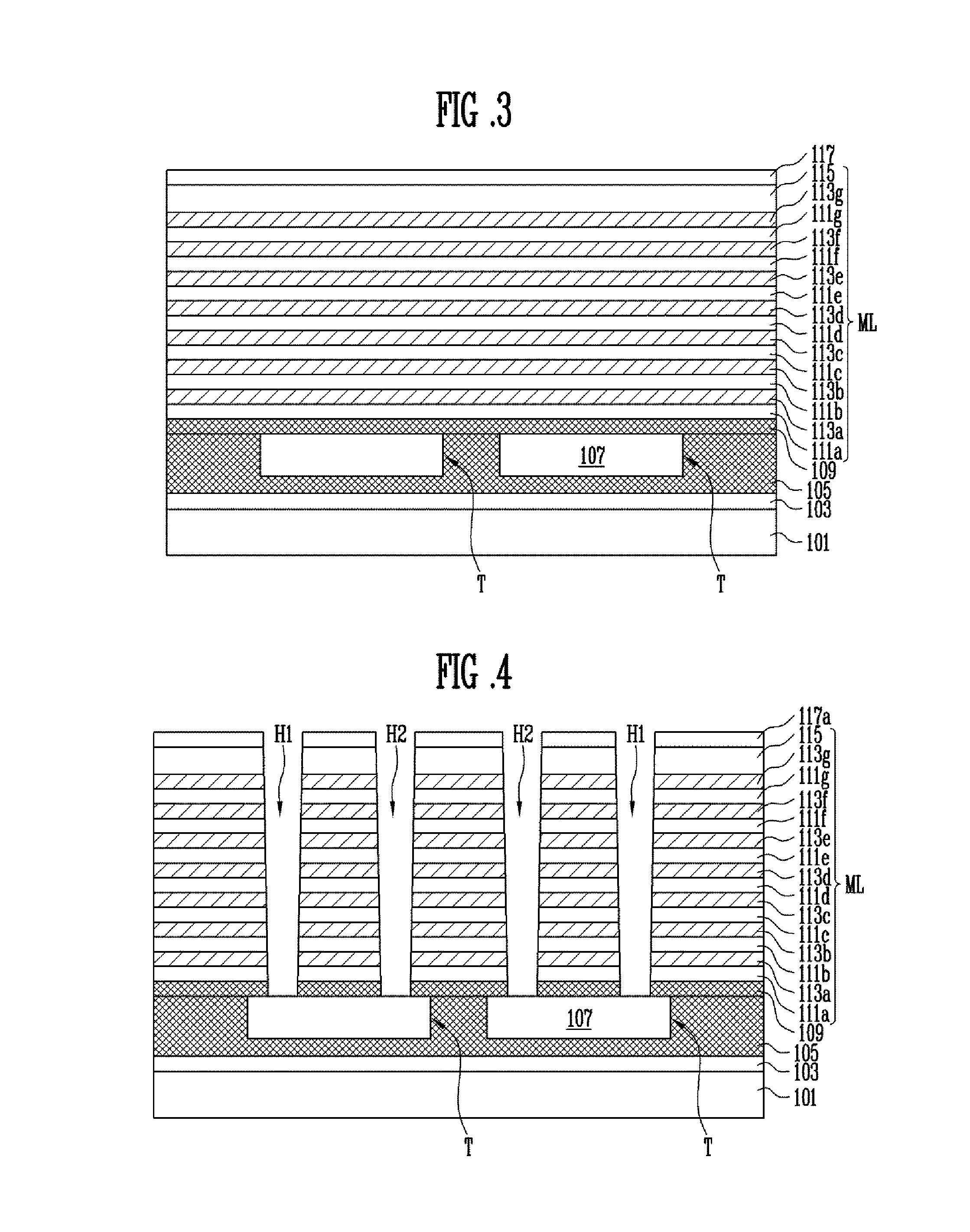
[0019]FIGS. 2 to 14 are cross-sectional views illustrating a method of manufacturing a three-dimensional (3-D) non-volatile memory device according to an embodiment of the present invention.

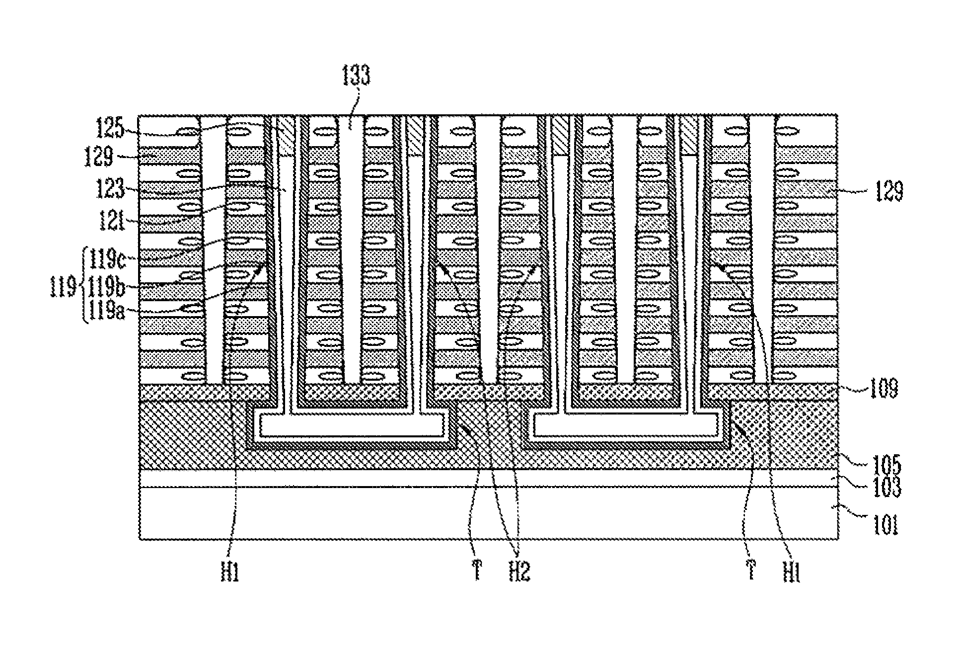
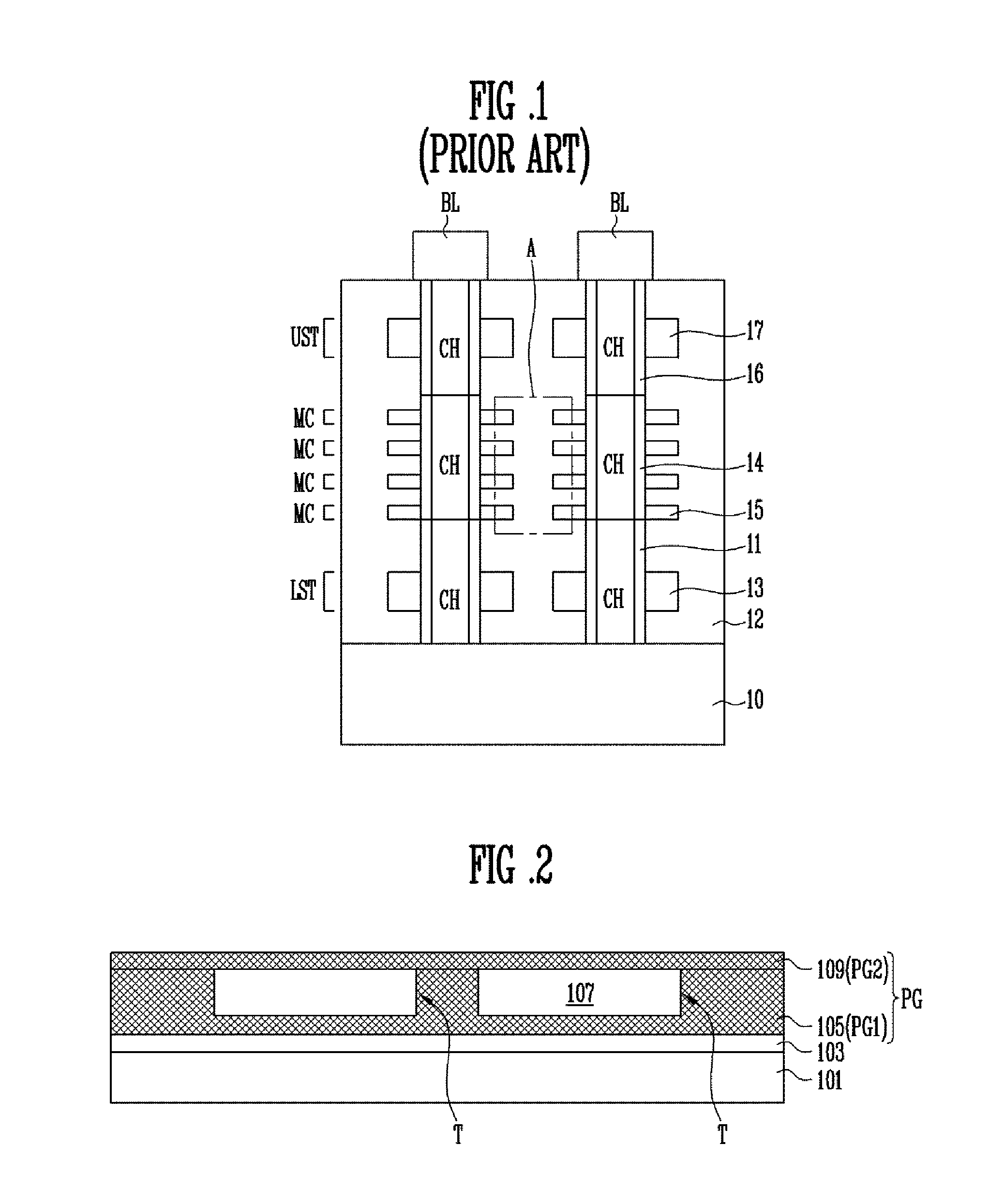
[0020]Referring to FIG. 2, a first interlayer insulating layer 103 may be formed over a substrate 101. Subsequently, a pipe gate PG that has first sacrificial layers 107 embedded therein may be formed on the firs...


PUM


Abstract

A three-dimensional (3-D) non-volatile memory device includes a plurality of vertical channel layers protruding from a substrate, a plurality of interlayer insulating layers and a plurality of memory cells stacked alternately along the plurality of vertical channel layers, and an air gap formed in the plurality of interlayer insulating layers disposed between the plurality of memory cells, so that capacitance between word lines is reduced to thus improve a program speed.

Description

CROSS-REFERENCE TO RELATED APPLICATION[0001]The present application claims priority to Korean patent application number 10-2011-0133739 filed on Dec. 13, 2011, in the Korean Intellectual Property Office, the entire disclosure of which is incorporated by reference herein.BACKGROUND[0002]1. Field of Invention[0003]The present invention relates generally to a semiconductor device and a method of manufacturing the same and, more particularly, to a three-dimensional non-volatile memory device, a memory system including the same and a method of manufacturing the same.[0004]2. Related Art[0005]A non-volatile memory device retains data even in the absence of a power supply. Two-dimensional memory devices in which memory cells are fabricated in a single layer over a silicon substrate are reaching physical limits, preventing higher levels of integration. Accordingly, three-dimensional non-volatile memory devices in which memory cells are stacked in a vertical direction over a silicon substrat...

Claims


Application Information

Patent Timeline
Patent Type & Authority Patents(United States)
IPC IPC(8): H01L27/115
CPCH01L27/11568H01L27/11582H10B43/30H10B43/27H01L21/76205H01L27/0688H10B43/20
Inventor BAEK, YONG MOOKAHN, JUNG RYUL
Owner SK HYNIX INC
Why Eureka
Try Eureka