Metal assisted chemical etching to produce III-V semiconductor nanostructures

a technology of metal-assisted chemical etching and nanostructures, which is applied in the direction of sustainable manufacturing/processing, final product manufacturing, paper/cardboard articles, etc., can solve the problems of hardly being able to offer complete control over the pattern and quality of nanostructures in an affordable and timely manner, and the macetching of other materials such as iii-v materials to produce periodic nanostructures has hardly been explored

Active Publication Date: 2015-02-10
THE BOARD OF TRUSTEES OF THE UNIV OF ILLINOIS
View PDF2 Cites 20 Cited by
  • Summary
  • Abstract
  • Description
  • Claims
  • Application Information

AI Technical Summary

Problems solved by technology

Many different fabrication methods can be used to produce nanostructures, but they generally have not been able to offer complete control over the pattern and quality of the nanostructures in an affordable and timely manner.
However, this can result in intense damage to the crystal structure and surface morphology.
However, MacEtch of other materials, such as III-V materials to produce periodic nanostructures, has hardly been explored and has not been effective in producing high aspect ratio nanostructures.

Method used


Image

  • Metal assisted chemical etching to produce III-V semiconductor nanostructures
  • Metal assisted chemical etching to produce III-V semiconductor nanostructures
  • Metal assisted chemical etching to produce III-V semiconductor nanostructures

Examples


Embodiment Construction

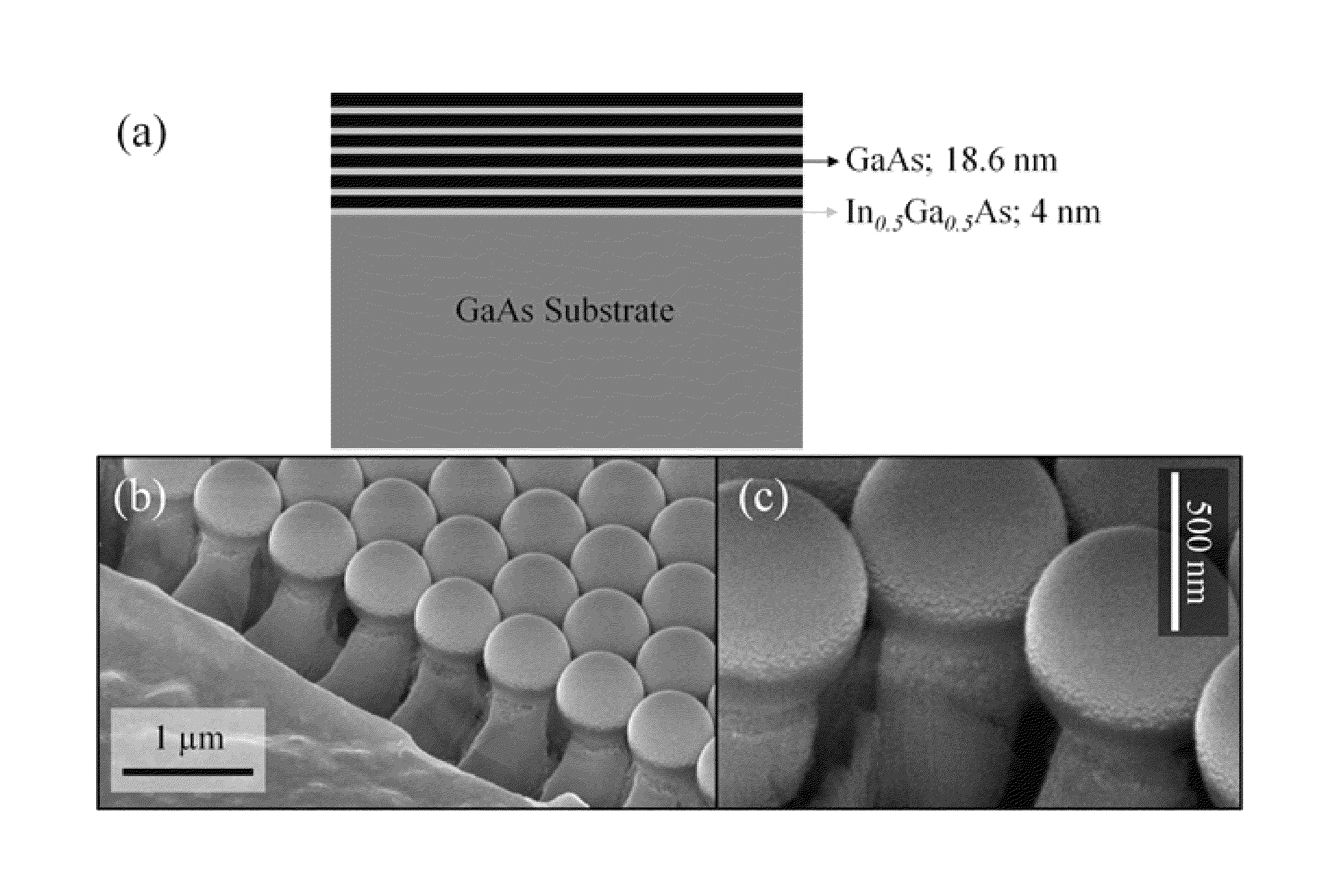
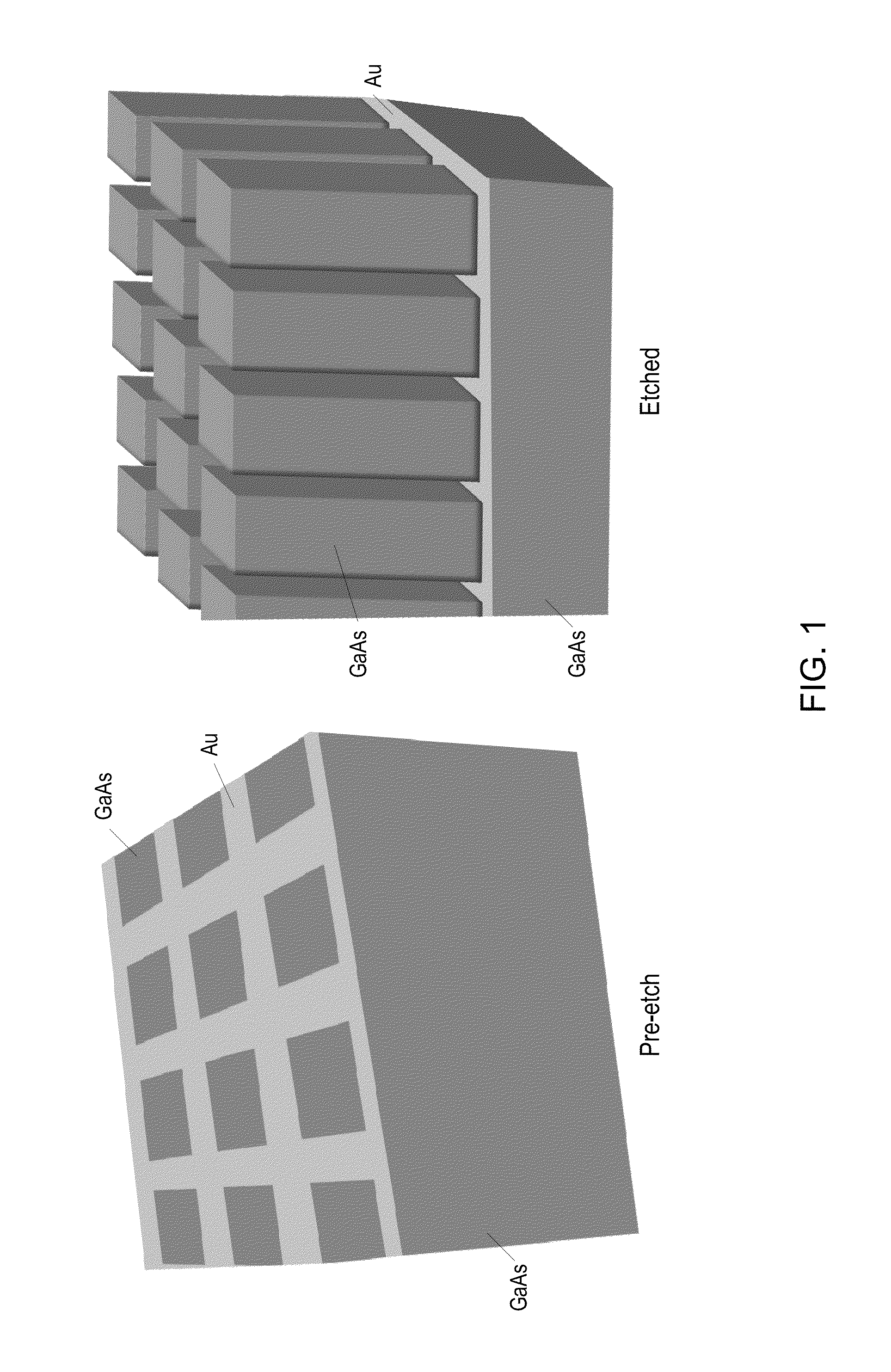
[0031]Methods of etching semiconductors such as III-V semiconductors to form semiconducting structures with nanometer dimensions are described herein. Etched arrays of III-V nanostructures can offer a variety of advantages over silicon because of the ability to create direct band gap, ternary, and heterostructure materials. In certain examples described below, periodic, high aspect ratio GaAs nanopillars are formed with lateral dimensions (e.g., widths or diameters) in the range of about 10 to about 1000 nm or about 500 to about 1000 nm by an etching method that may be referred to as metal assisted chemical etching (MacEtch). When overlaid with a metal (e.g., gold) pattern and exposed to an acidic environment with a suitable oxidizing agent, the GaAs directly underneath the metal pattern etches. A metal assisted chemical etching process had previously been proven for silicon, but prior to this work, such a method had not been successfully applied to III-V semiconductors.

[0032]The me...


PUM

PropertyMeasurementUnit
temperatureaaaaaaaaaa
diametersaaaaaaaaaa
diametersaaaaaaaaaa

Abstract

Methods of metal assisted chemical etching III-V semiconductors are provided. The methods can include providing an electrically conductive film pattern disposed on a semiconductor substrate comprising a III-V semiconductor. At least a portion of the III-V semiconductor immediately below the conductive film pattern may be selectively removed by immersing the electrically conductive film pattern and the semiconductor substrate into an etchant solution comprising an acid and an oxidizing agent having an oxidation potential less than an oxidation potential of hydrogen peroxide. Such methods can form high aspect ratio semiconductor nanostructures.

Description

RELATED APPLICATIONS[0001]This application claims priority under 35 U.S.C. §119(e) to U.S. Provisional Application No. 61 / 625,905, “METAL ASSISTED CHEMICAL ETCHING TO PRODUCE III-V SEMICONDUCTOR NANOSTRUCTURES,” filed Apr. 18, 2012, the entire contents of which are incorporated by reference.FEDERALLY FUNDED RESEARCH OR DEVELOPMENT[0002]The invention described herein was made with government support under contract number CMMI0749028 awarded by the National Science Foundation. The U.S. Government has certain rights in this invention.TECHNICAL FIELD[0003]The present disclosure is related generally to etching semiconducting materials and more particularly to metal-assisted chemical etching to form nanostructures.BACKGROUND[0004]Nanostructures formed from semiconducting materials are becoming more prevalent. Many different fabrication methods can be used to produce nanostructures, but they generally have not been able to offer complete control over the pattern and quality of the nanostru...

Claims


Application Information

Patent Timeline
Patent Type & Authority Patents(United States)
IPC IPC(8): C03C15/00H01L21/306H01L31/18H01L33/00H01L33/20
CPCH01L21/30612H01L33/0062H01L31/184Y10S977/762H01L33/20Y02P70/50Y02E10/544
Inventor LI, XIULINGDEJARLD, MATTHEW T.SHIN, JAE CHEOLCHERN, WINSTON
Owner THE BOARD OF TRUSTEES OF THE UNIV OF ILLINOIS
Why Eureka
Try Eureka