Eureka AIR delivers breakthrough ideas for toughest innovation challenges, trusted by R&D personnel around the world.

Method and device for producing a semiconductor layer

Active Publication Date: 2015-02-17
OC3 AG
View PDF10 Cites 0 Cited by
  • Summary
  • Abstract
  • Description
  • Claims
  • Application Information

AI Technical Summary

Benefits of technology

[0017]A significant advantage of the invention is the fact that the excitation and/or ionization of all metallic and chalcogen components required for the layer formation result in an improvement of the structural and therefore of the electrical layer qualities of the deposited absorber layer. The improving of the electrical layer qualities achieves an efficiency of the solar cells that is increased by 10%. Compared to a pure co-evaporation process an efficiency increase of approximately 35% is achieved. Thus, the yield of the solar cell can be decisively increased while retaining the same absorber surface. Another advantage is the use of only one single wide-beam ion source in the coating chamber. Thus, the costs for investment, regulation and control are di

Problems solved by technology

The rate (i.e. evaporation rate) as well as the ion current density of these sources are very low and therefore not suitable for the layer deposition on an industrial scale.
Therefore, on the one hand a deposition on temperature-sensitive substrates (such as, for example, polyimide sheet), that can therefore only be heated to a low extent is not possible or only possible with a considerably lesser efficiency of the solar cells.
On the other hand, high energy costs accumulate during the production of the Cu(In,Ga)Se2 absorber layers on account of the high substrate temperatures.
The simultaneous excitation and/or ionization of all layer-forming components (Cu, In, Ga, Se) in the coating chamber by means of an additional plasma excitation can only partially solve this problem.
As the reactivity of the layer-forming elements is elevated, however, an additional, non-thermal energy contribution into the growing Cu(In,Ga)Se2 layer cannot take place on account of the low energy of the ionized and/or excited particles of only a few eV i.e., high substrate temperatures continue to be required for a sufficiently good crystal quality.
A further disadvantage of this process is the fact that as a result of the homogenous mixing of the metallic vapors and chalcogenic vapors the adj

Method used


Image

  • Method and device for producing a semiconductor layer
  • Method and device for producing a semiconductor layer

Examples


Example

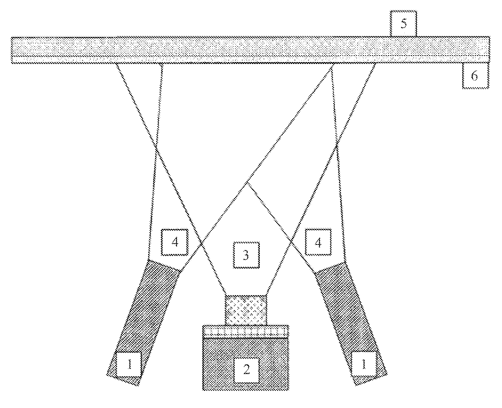
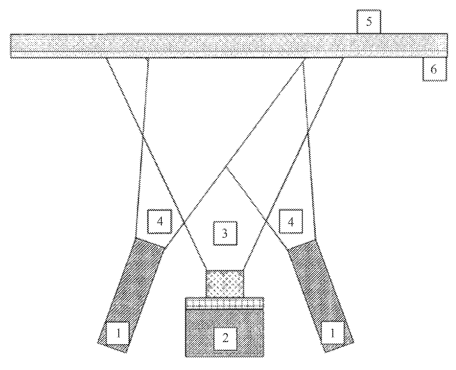
DETAILED DESCRIPTION OF THE DRAWINGS

[0020]The invention is explained in the following using an exemplary embodiment.

[0021]Example of a Procedure of a Method

[0022]A substrate 5 provided with a molybdenum back contact 6 is placed into the coating chamber. The layer thickness of the molybdenum back contact 6 is in the range between 0.5 and 2 μm.

[0023]Now, a Cu(In,Ga)Se2 semiconductor layer is applied in a vacuum process at a pressure between 1·10−6 and 1·10−4 mbar onto the metallic back contact 6. The metallic components from metallic evaporator sources 1 are evaporated at a rate ratio of 0.813 from a low-energy broad-beam ion source 2. The energy of the selenium ions can be selected in the range between 10 and 500 eV.

[0024]The substrate holder is heated in this coating step to a temperature between 400 and 550° C.

[0025]An overlapping of the metal vapor beams and of the selenium ion beam is achieved by the alignment of the metal evaporator 1 and of the beam guidance 4 resulting from it...


PUM

PropertyMeasurementUnit
Temperatureaaaaaaaaaa
Pressureaaaaaaaaaa
Pressureaaaaaaaaaa

Abstract

The invention relates to a method and a device for producing a semiconductor layer. The problem addressed is that of increasing the deposition rate of the layer constituents and significantly improving the efficiency of a resulting solar cell. At the same time, the material costs are intended to be reduced. The problem is solved by virtue of the fact that, in a vacuum chamber, metal evaporator sources release Cu, In and/or Ga or the chalcogenide compounds, the latter are focused as metal vapor jets onto the substrate, and Se and/or S emerge(s) in an ionized fashion from a chalcogen low-energy wide-beam ion source and this beam is focused onto the surface of the substrate in such a way that it overlaps the metal vapor jets. A device for carrying out the method is described.

Description

CROSS-REFERENCE TO RELATED APPLICATIONS[0001]This application is a 371 U.S. National Stage of International Application No. PCT / EP2010 / 001093, filed Feb. 22, 2010, the disclosure of which is incorporated herein by reference.FIELD OF THE INVENTION[0002]The invention relates to a method and a device for depositing a chalcopyrite absorber layer for thin layer solar cells on a layer system in a vacuum process, whereby a special low-energy broad-beam ion source is used for the production. The development of highly efficient solar cells as well as their economical production are main goals of photovoltaic. In the course of this development thin-layer solar cells are becoming more and more significant and will open up larger areas of the market in the future that is currently dominated by crystalline silicon solar cells.BACKGROUND OF THE INVENTION[0003]A promising absorber material for use in thin-layer solar cells is the material system of the chalcopyrite semiconductors I-IIII-VI2 with t...

Claims


Application Information

Patent Timeline
IPC IPC(8): H01L21/00C23C14/00C23C14/06H01L21/02H01L31/032H01L31/0749
CPCH01L31/0749C23C14/0031C23C14/0623H01L21/02491H01L21/02568H01L21/02631H01L31/0322Y02E10/541Y02P70/50
Inventor ZACHMANN, HENDRIKOTTE, KARSTENNEUMANN, HORSTSCHOLZE, FRANKPISTOL, LUTZ
Owner OC3 AG
Why Eureka
Eureka Blog
Learn More