Graphene field effect transistor

a graphene field effect transistor and transistor technology, applied in transistors, nanoinformatics, solid-state devices, etc., can solve the problems of very low graphene resistivity, meet scientific and technical limits,

Inactive Publication Date: 2015-02-17
IBM CORP
View PDF38 Cites 19 Cited by
  • Summary
  • Abstract
  • Description
  • Claims
  • Application Information

AI Technical Summary

Problems solved by technology

However, it is believed this approach will soon meet both scientific and technical limits, and there have been tremendous efforts to seek alternative device technologies.
Moreover, graphene resistivity is very low, e.g., less than the resistivity of silver, which is the lowest resistivity substance currently known at room temperature.

Method used


Image

  • Graphene field effect transistor
  • Graphene field effect transistor
  • Graphene field effect transistor

Examples


Embodiment Construction

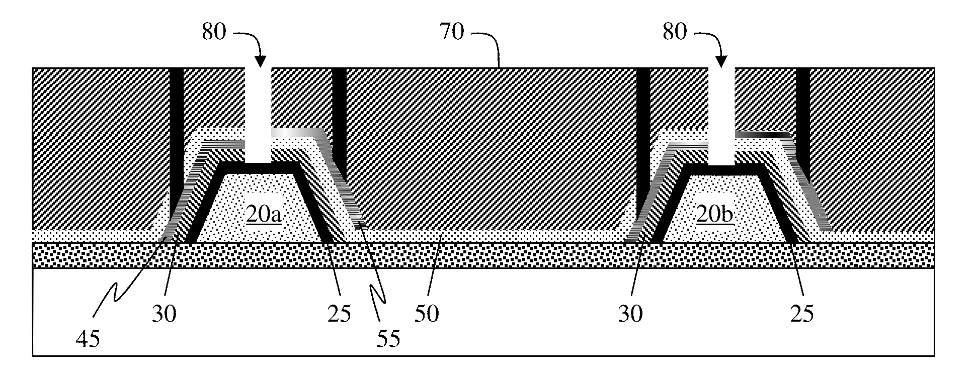
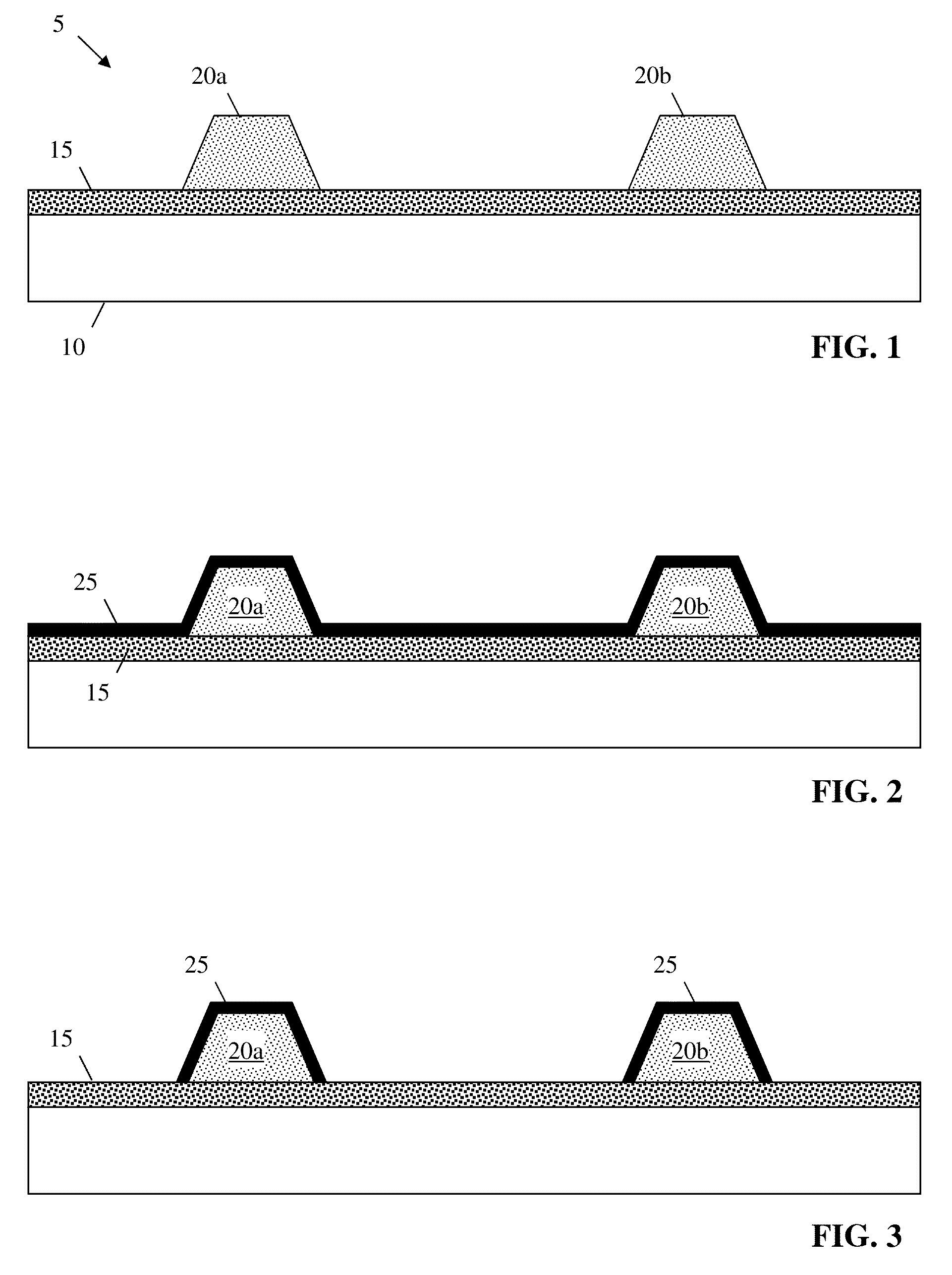
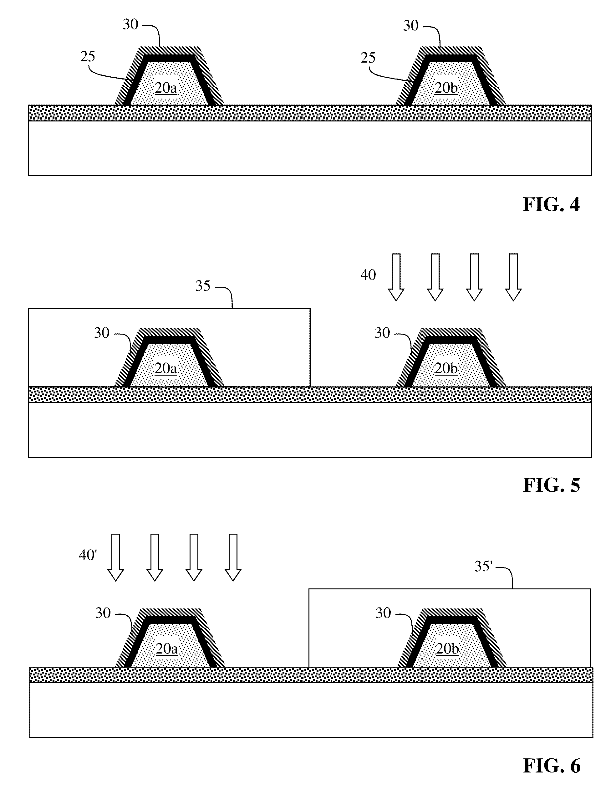
[0013]The invention relates to semiconductor structures and methods of manufacture and, more particularly, to a graphene field effect transistor (FET). According to aspects of the invention, graphene that functions as a channel in a FET is grown on a sacrificial material that is arranged on sidewalls of a mandrel. In embodiments, source / drain electrodes, a gate dielectric, and a gate electrode are formed on the graphene, and the sacrificial material is subsequently removed. In this manner, a vertical graphene FET is formed at the wafer level without using transfer processes.

[0014]Graphene is currently being used in field effect transistors (FETs) and integrated circuits (ICs). However, single sheets of graphene are difficult to produce, and more difficult to form on an appropriate substrate. For example, graphene is typically utilized by growing the graphene on a first substrate and then transferring the graphene to a second substrate, e.g., referred to as exfoliation, transfer, etc...


PUM


Abstract

Manufacturing a semiconductor structure including: forming a seed material on a sidewall of a mandrel; forming a graphene field effect transistor (FET) on the seed material; and removing the seed material.

Description

FIELD OF THE INVENTION[0001]The invention relates to semiconductor structures and methods of manufacture and, more particularly, to a graphene field effect transistor (FET).BACKGROUND[0002]In the last few decades, the semiconductor industry has been able to maintain steady improvements of device performance by the scaling of silicon-based devices. However, it is believed this approach will soon meet both scientific and technical limits, and there have been tremendous efforts to seek alternative device technologies. One such alternative is the use of graphene in semiconductor structures.[0003]Graphene is a layer of carbon atoms bonded in a honeycomb crystal lattice. Graphene has a high carrier mobility, as well as low noise, allowing it to be used as a substitute for silicon in the channel in a FET. Intrinsic graphene is a semi-metal or zero-gap semiconductor, with an E-k relation that is linear at low energies near the six corners of the two-dimensional hexagonal Brillouin zone, lea...

Claims


Application Information

Patent Timeline
Patent Type & Authority Patents(United States)
IPC IPC(8): H01L21/00H01L27/12H01L29/16H01L29/417H01L29/66H01L29/778H01L29/78H01L29/786
CPCH01L29/1606H01L29/78H01L29/66045H01L29/778H01L29/41733H01L29/66742H01L29/78684H01L29/78696H01L27/1222H01L29/7786B82Y10/00B82Y30/00B82Y40/00C01B32/186H01L29/42384H01L29/785
Inventor ADKISSON, JAMES W.DUNBAR, THOMAS J.GAMBINO, JEFFREY P.LEITCH, MOLLY J.
Owner IBM CORP
Why Eureka
Try Eureka