Electronic MEMS device comprising a chip bonded to a substrate and having cavities and manufacturing process thereof

a technology of electronic mems and chip, which is applied in the direction of microstructural technology, decorative arts, chemical vapor deposition coating, etc., can solve the problems of chip b>1/b> tilting and glue layer delamination, low assembly process yield, even lower than 50%

Inactive Publication Date: 2015-03-17
STMICROELECTRONICS SRL
View PDF11 Cites 5 Cited by
  • Summary
  • Abstract
  • Description
  • Claims
  • Application Information

AI Technical Summary

Benefits of technology

[0014]In practice, in the support, underneath the area of the chip where the cavities are formed, there is a depressed portion containing part of the glue. During the thermal treatments, the glue, being compliant, allows for expansion of the air in the cavities within the depressed area, thus preventing raising and / or tilting of the chip with respect to the substrate. Typically, the depressed portion comprises a recess formed by the surface layers of the support. In addition, spacer elements may extend within the glue layer so as to ensure the thickness of the swelling to be always smaller than the distance between the chip and the plane underlying the chip itself and to ensure planarity of the chip.

Problems solved by technology

This type of attachment entails, however, problems.
Swellings are thus created that tend to raise the chip and, in particular in presence of lack of uniformity, can cause tilting of the chip 1 and delaminating of the glue layer.
The consequence thereof is that the yield of the assembly process is low, even lower than 50%.
The same problem applies to other types of MEMS devices, having cavities closed by sealing layers of compliant material and / or bonded on areas of compliant material.

Method used


Image

  • Electronic MEMS device comprising a chip bonded to a substrate and having cavities and manufacturing process thereof
  • Electronic MEMS device comprising a chip bonded to a substrate and having cavities and manufacturing process thereof
  • Electronic MEMS device comprising a chip bonded to a substrate and having cavities and manufacturing process thereof

Examples


Embodiment Construction

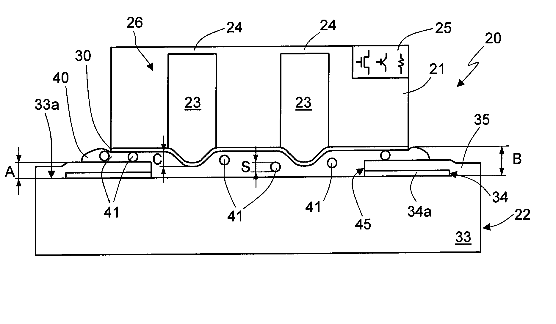
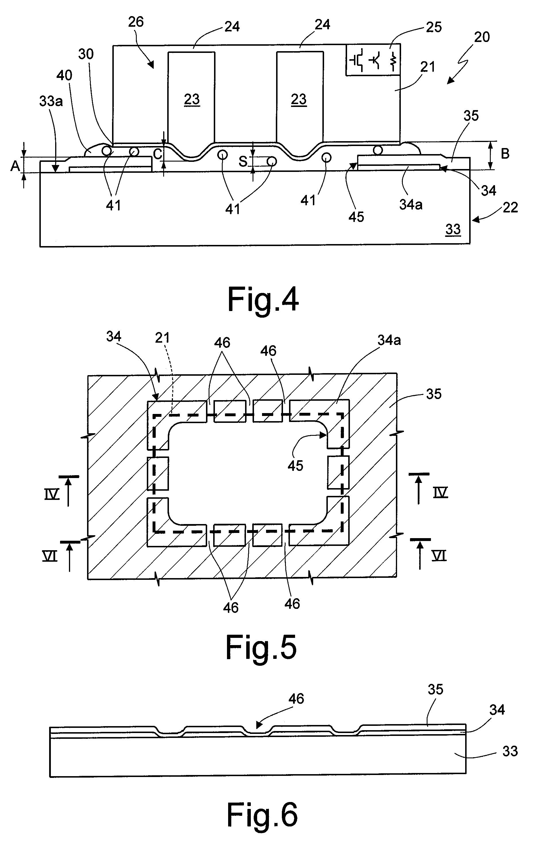
[0023]FIGS. 4-6 show an electronic device 20 including a chip 21 bonded to a substrate 22 by a glue layer 40. The chip 21 has cavities 23 extending from the rear surface of the chip 21 and delimiting membranes 24 at the bottom. If the electronic device 20 forms part of a chemical sensor, adsorbent layers (not shown) may be formed on the membranes 24 and may be of a material able to bind with the chemical substance to be detected, as described in detail in aforementioned patent application U.S. patent application Ser. No. 12 / 648,996. For example, the adsorbent layers can contain metal-porphyrins having an affinity with the chemical matters to be detected and form, together with the membranes 24, a sensitive area 26. For the rest, the chip 21 may comprise a circuitry area 25 including electronic components (shown schematically) so as to form, with the sensitive area 26, a device for detecting chemical matters, for example, odorous chemical matters.

[0024]An adhesive film 30 covers the ...


PUM

PropertyMeasurementUnit
depthaaaaaaaaaa
depthaaaaaaaaaa
widthaaaaaaaaaa

Abstract

An electronic MEMS device is formed by a chip having with a main face and bonded to a support via an adhesive layer. A cavity extends inside the chip from its main face and is closed by a flexible film covering the main face of the chip at least in the area of the cavity. The support has a depressed portion facing the cavity and delimited by a protruding portion facing the main face of the chip. Inside the depressed portion, the adhesive layer has a greater thickness than the projecting portion so as to be able to absorb any swelling of the flexible film as a result of the expansion of the gas contained inside the cavity during thermal processes.

Description

BACKGROUND[0001]1. Technical Field[0002]The present disclosure relates to an electronic micro-electro-mechanical system (MEMS) device comprising a chip bonded to a substrate and having cavities and to the manufacturing process thereof. In particular, the present disclosure applies to chemical sensors for detecting odorous matters.[0003]2. Description of the Related Art[0004]As is known, in devices for recognizing odorous matters (such as the one described, for example, in U.S. patent application Ser. No. 12 / 648,996, published as U.S. Application Publication No. 2010 / 0170324, and incorporated herein by reference in its entirety) the semiconductor material chip accommodates one or more cavities delimiting respective membranes carrying, i.a., respective adsorbent layers. Each membrane and the respective adsorbent layer form part of an oscillating circuit having electrical characteristics that vary with the weight of the ensemble including the membrane, the adsorbent layer, and any poss...

Claims


Application Information

Patent Timeline
Patent Type & Authority Patents(United States)
IPC IPC(8): H01L29/84H01L21/02B81C1/00
CPCB81C1/00182G01N2291/0256B81C2203/032B81C2203/019B81B2201/0214
Inventor ZIGLIOLI, FEDERICO GIOVANNI
Owner STMICROELECTRONICS SRL
Why Eureka
Try Eureka