Packaging structure of a micro-device including a getter material

a technology of micro-devices and packaging structures, applied in micro-structural devices, fluid speed measurement, instruments, etc., can solve the problems of affecting the quality of the produ

Active Publication Date: 2015-03-17
COMMISSARIAT A LENERGIE ATOMIQUE ET AUX ENERGIES ALTERNATIVES
View PDF26 Cites 1 Cited by
  • Summary
  • Abstract
  • Description
  • Claims
  • Application Information

AI Technical Summary

Benefits of technology

[0015]Unlike packaging structures of prior art, the layer of getter material thus extends at the bonding interface between both substrates, which has many advantages in particular for making the bonding interface which consists of at least one metal, that is the getter material.
[0017]Such a packaging structure does not require the implementation of steps of shaping the getter material, which reduces the packaging structure cost.
[0018]Moreover, as compared with the packaging structures including discretized portions of getter material, the area of getter material exposed in the cavity is increased, which provides a larger pumping capacity, or, for the same desired pressure, relaxation of constraints to obtain the pumping capacity required to achieve this pressure.
[0025]The bonding interface may include at least one heat-compressed dielectric portion against the layer of getter material or against at least one metal portion provided on the layer of getter material. A part of the layer of getter material may form the bonding interface. In this case, the bonding interface may include at least one metal portion and a dielectric portion, for example comprising semi-conductor oxide or nitride (such as SiO2 and / or SiN), heat-compressed against each other. The thermal activation of the getter deposited onto the second substrate, being implemented during the assembling process, helps to create a getter / dielectric connection when the dielectric portion is made integral with the layer of getter material.
[0031]It is thus possible to make a via passing through the first substrate and which is electrically connected to the getter. Such a via enables the getter to be biased to then play a role in the operation of the micro-device or even to electrically connect it to an electrical potential or to the ground.
[0042]In this case, the first metal portion may be made by electrolytically depositing at least one metal material on the layer of getter material during which a current capable of growing said metal material flows in the layer of getter material. The electrolytic growth of the metallic material (eg Au—Sn if a solder metal is desired) can lead to the formation of a strong metal / metal interface. In addition, the electrolytic deposition of the metallic material may have a thickness of several microns (eg up to 10 microns) which allows to simultaneously define the height of the cavity and prevent to achieve before a hollow in the cap.

Problems solved by technology

In any case, these shaping steps of the getter material represent a significant cost in making packaging structures.
Furthermore, the implementation of these steps presents a risk towards the getter material because of the chemical compatibility thereof with the product used for making this operation for discretizing the getter material.
Such a process has the drawback of involving the creation of openings through the cap to remove the sacrificial material on which the thin film(s) have been deposited.
Moreover, in this method, it is the backside (that is the side of the getter material that was deposited against the sacrificial material) of the layer of getter material which is exposed in the cavity, which does not allow for example to use a temperature adjustment sub-layer of the getter material.

Method used


Image

  • Packaging structure of a micro-device including a getter material
  • Packaging structure of a micro-device including a getter material
  • Packaging structure of a micro-device including a getter material

Examples


first embodiment

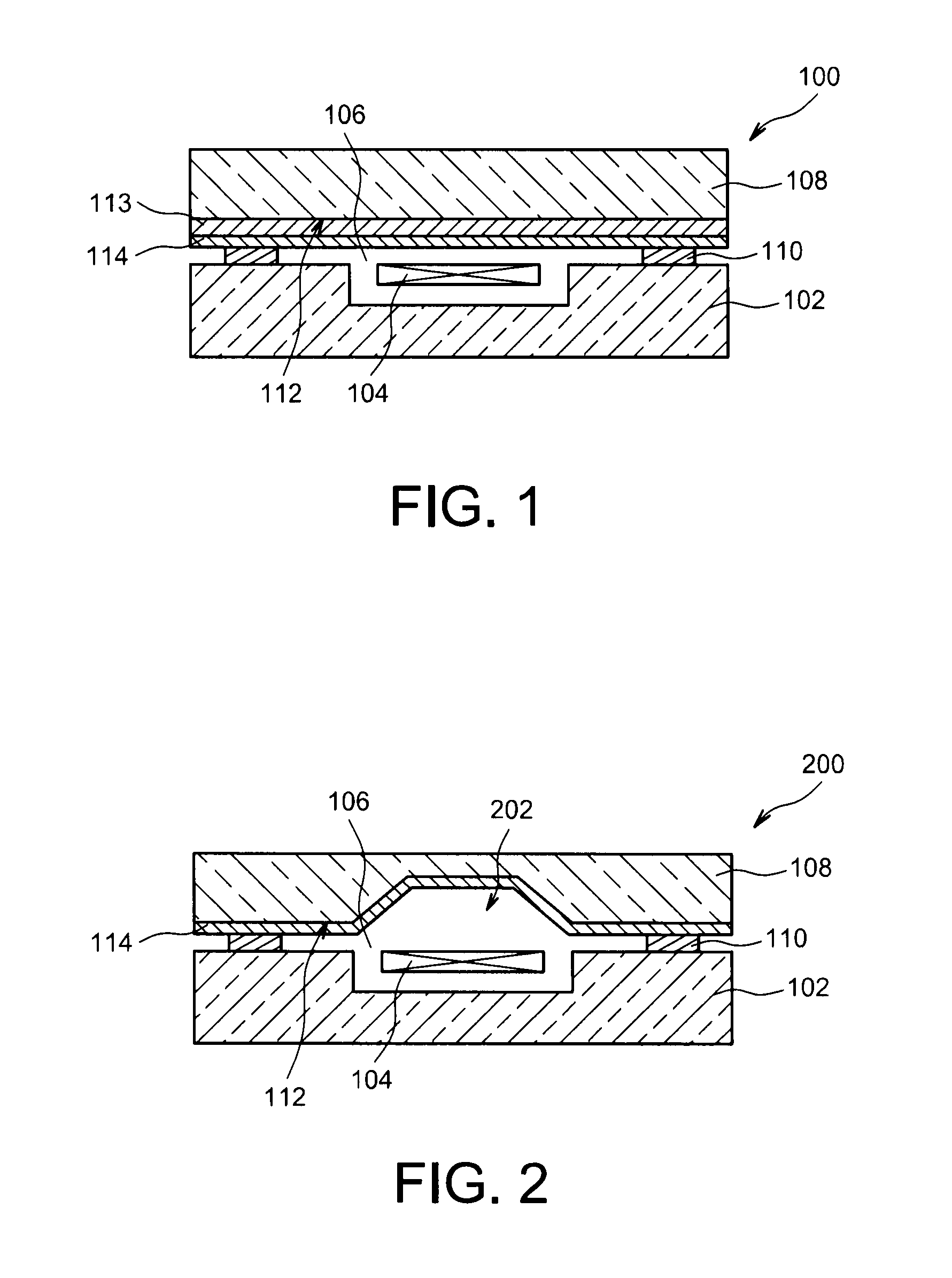
[0056]FIG. 1 which represents a packaging structure 100 will be referred to.

[0057]The packaging structure 100 includes a first substrate 102, for example comprising a semi-conductor such as silicon, wherein a micro-device 104 is made, for example of the MEMS and / or NEMS type or of the infrared detector type, such as a micro-bolometer. The micro-device 104 is packaged into a cavity 106 formed between the first substrate 102 acting as a support to the micro-device 104, and a second substrate 108, also comprising a semi-conductor such as silicon or glass, and forming a cap. The substrates 102 and 108 are made integral with each other through a bonding interface 110 made as a sealing bead. This sealing bead consists for example of one or more fusible materials.

[0058]An insulating layer 113 comprising for example oxide or nitride when the second substrate 108 includes a semi-conductor or electrically conducting material, is made at a main face 112 of the second substrate 108. This insul...

second embodiment

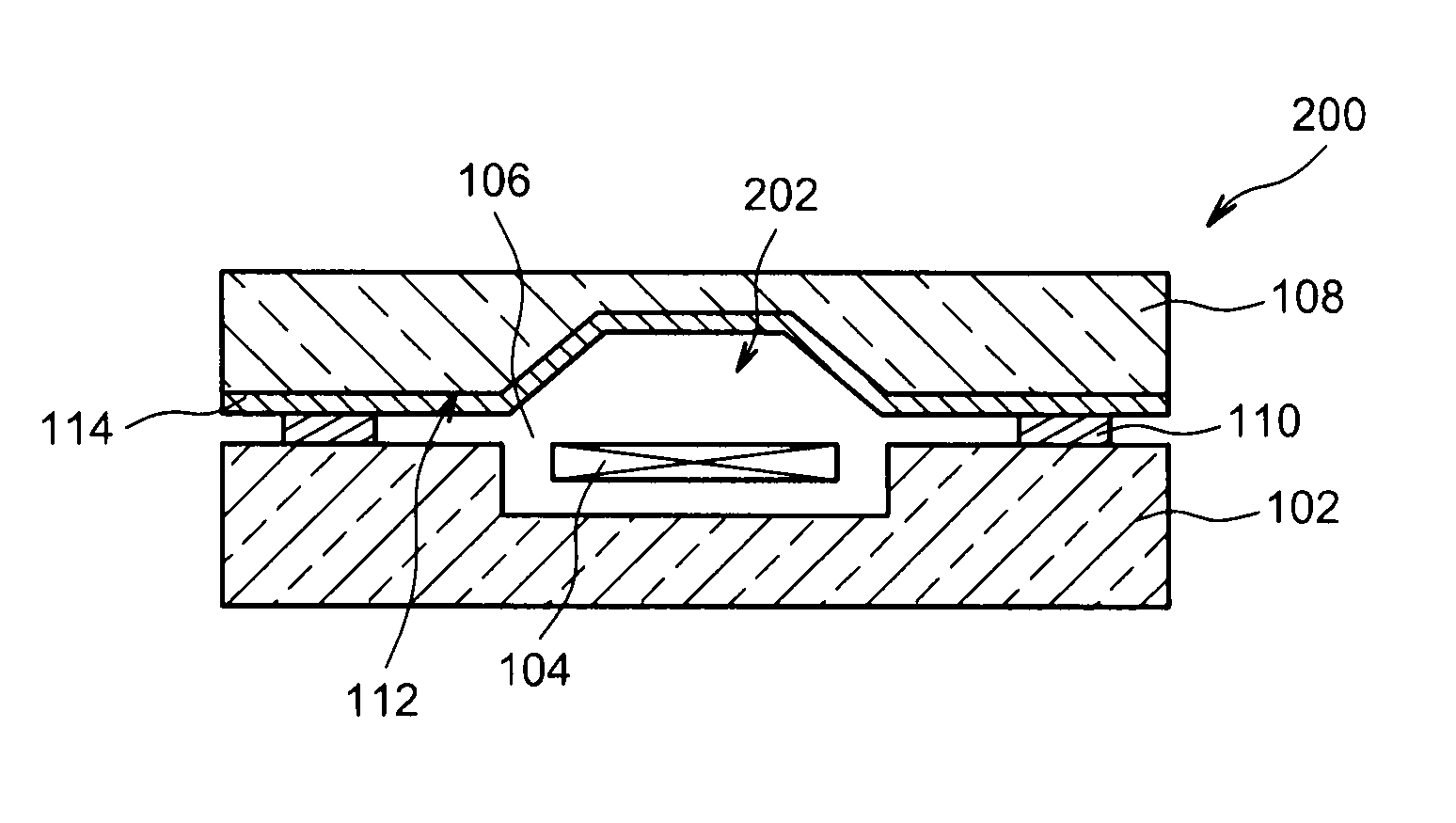
[0061]FIG. 2 which represents a packaging structure 200 will be referred to.

[0062]Different from the previously described structure 100, a hole, or trough 202 is formed in the second substrate 108, at the main face 112 of the second substrate 108. This trough 202 is formed in a part of the second substrate 108 intended to be provided in the cavity 106. This trough 202 is formed prior to depositing the layer of getter material 114 in order that the whole main face 112 and the walls of the trough 202 are covered with the layer of getter material 114. Moreover, different from the structure 100 according to the first embodiment, the packaging structure 200 does not include an insulating layer provided between the main face 112 of the second substrate 108 and the layer of getter material 114.

[0063]As compared with the first embodiment, such a trough 202 enables to increase the volume of the cavity 106 wherein the micro-device 104 is packaged. This trough 202 is only made through a part ...

third embodiment

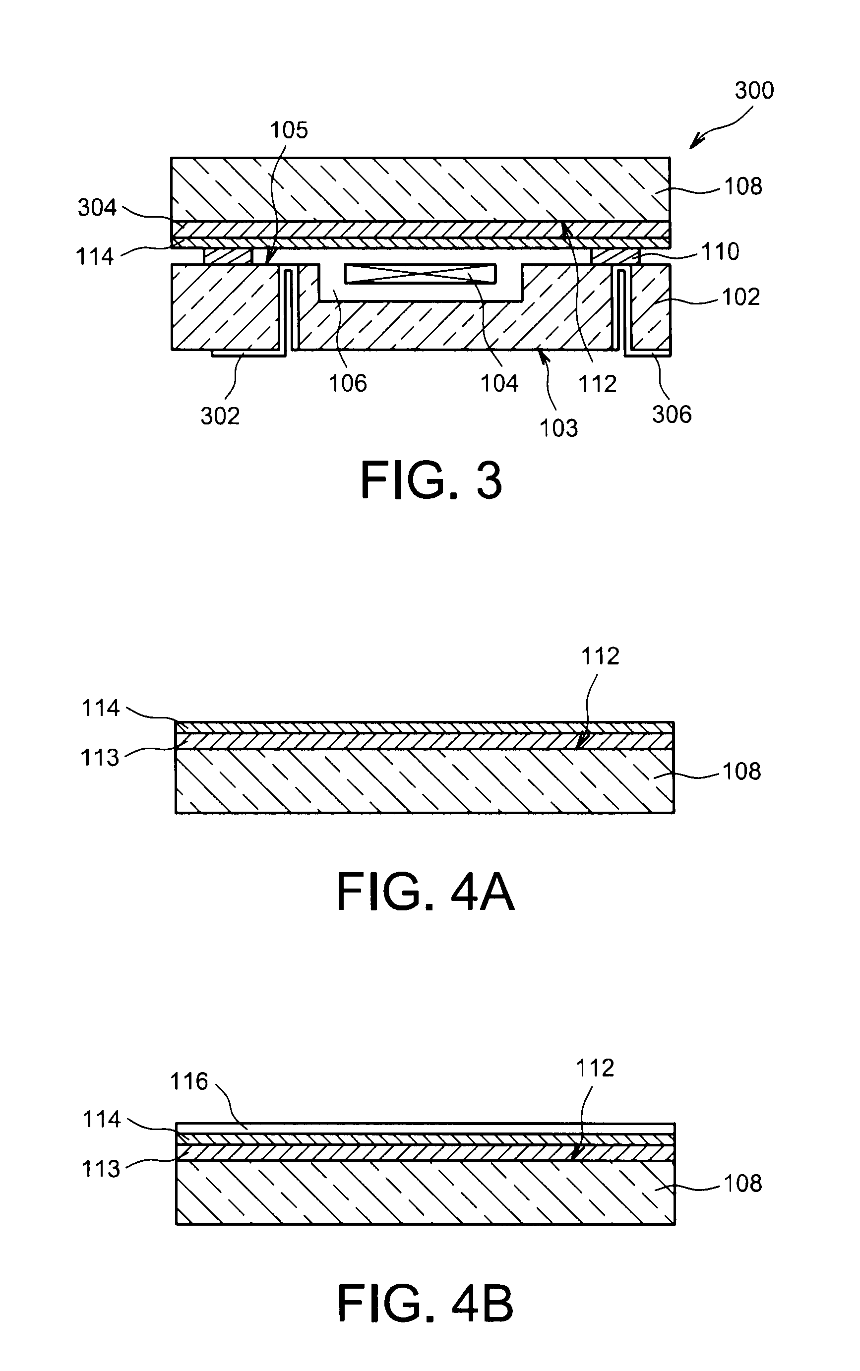
[0065]FIG. 3 which represents a packaging structure 300 will be referred to.

[0066]Different from the previously described structure 100, a through via 302 is formed through the first substrate 102, from a back face 103 of the first substrate 102 opposed to a front face 105 of the first substrate 102 at which the micro-device 104 is made. This through via 302 opens into the cavity 106 and is electrically connected to the micro-device 104, thus forming an electrical access to the micro-device 104 from the back face 103 of the first substrate 102. A via 306, electrically connected to the getter material 114 via the bonding interface 110, is made through the first substrate 102, and thus forms an electrical access to the getter material 114 from the back face 103 of the first substrate 102. Other vias, not represented and similar to the via 302 or via 306, may be formed through the first substrate 102. Such a via 302 enables to perform an electrical contact of the micro-device 104 at t...


PUM

PropertyMeasurementUnit
thicknessaaaaaaaaaa
thicknessaaaaaaaaaa
thicknessaaaaaaaaaa

Abstract

A packaging structure including at least one cavity wherein at least one micro-device is provided, the cavity being bounded by at least a first substrate and at least a second substrate integral with the first substrate through at least one bonding interface consisting of at least one metal or dielectric material, wherein at least one main face of the second substrate provided facing the first substrate is covered with at least one layer of at least one getter material, the bonding interface being provided between the first substrate and the layer of getter material.

Description

TECHNICAL FIELD[0001]This invention relates to the field of structures for packaging micro-devices including getter materials used for absorbing and / or adsorbing gases in a closed environment.[0002]The invention is in particular applicable to packaging of micro-devices including one or more microsystems, for example of the MEMS (electromechanical microsystems) and / or NEMS (electromechanical nanosystems) type or of the infrared detector type, such as micro-bolometers.[0003]The invention more particularly relates to a structure for hermetically packaging under a controlled atmosphere resonating MEMS type micro-devices.STATE OF PRIOR ART[0004]Some microsystems such as those of MEMS and / or NEMS type, or infrared micro-detectors, require to be packaged in a cavity under controlled atmosphere (type of gas and pressure within the cavity) to be in a good working order.[0005]The technology used theretofore to achieve such packaging consists in first making these microsystems collectively on ...

Claims


Application Information

Patent Timeline
Patent Type & Authority Patents(United States)
IPC IPC(8): H01L23/20H01L21/322B81B7/00H01L23/26H01L23/31
CPCH01L23/26H01L23/315B81B7/0038H01L2924/0002H01L2924/00
Inventor BAILLIN, XAVIERFERRANDON, CHRISTINE
Owner COMMISSARIAT A LENERGIE ATOMIQUE ET AUX ENERGIES ALTERNATIVES
Why Eureka
Try Eureka