

Organic electroluminescent device
a technology of electroluminescent devices and electroluminescent tubes, which is applied in the manufacture of electrode systems, electric discharge tubes/lamps, and discharge tubes luminescent screens, etc., can solve the problems of oled devices that lose light, the loss factor of oled devices is particularly difficult to extract light in an economic way, and the light emitted in these modes is particularly difficult to be extracted. , to achieve the effect of low cost and easy manufacturing and reliabl
- Summary
- Abstract
- Description
- Claims
- Application Information
AI Technical Summary
Benefits of technology
Problems solved by technology
Method used
Image

Examples
example a
[0030]
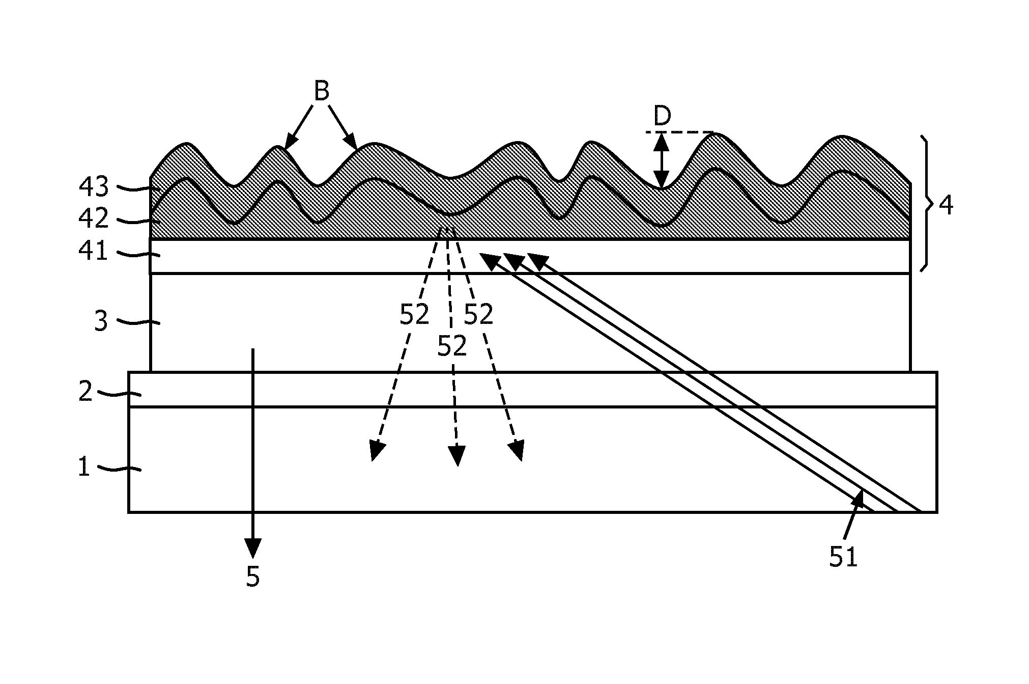
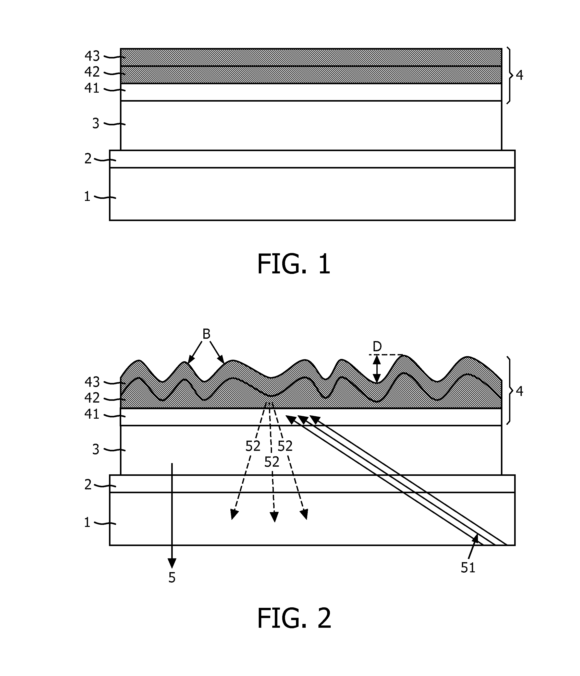
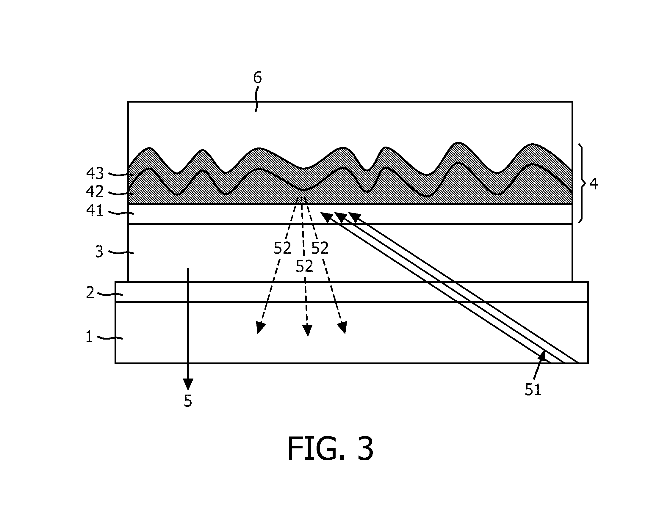
Layermateriald (nm)Tg (° C.)Substrate 1glassnon-organicFirst electrode 2ITO100non-organicOLE layer stack 3Spiro-TAD:F4-TCNQ 2%30133Spiro-TAD10133Spiro.TAD:Ir(mdq)2 acac301339%Bis-OXD10147Bis-OXD:W2(hpp)4 5%10147Protection layer 41WO360non-organicBuckling layer 42α-NPD:F4-TCNQ25 95Stress inducingAl20non-organiclayerCDL (optional)Al (or Co)80non-organic
[0031]In example A, Tg of the buckling layer is 38° C. lower than the lowest Tg of the organic-light-emitting layer stack.
example b
[0032]
Layermateriald (nm)Tg (° C.)Substrate 1glassnon-organicFirst electrode 2ITO100non-organicOLE layer stack 3Spiro-TAD:F4-TCNQ 2%30133Spiro-TAD10133Spiro.TAD:Ir(mdq)2 acac301339%Bis-OXD10147Bis-OXD:W2(hpp)4 5%10147Protection layer 41WO360non-organicBuckling layer 42TPD:F4-TCNQ25 60Stress inducingAl20non-organiclayerCDL (optional)Al (or Co)80non-organic
[0033]In this example B, Tg of the buckling layer is 73° C. lower than the lowest Tg of the organic-light-emitting layer stack.
[0034]In the examples A and B, Bis-OXD denotes 4,4′-bis(5-phenyl-[1,3,4]oxadiazol-2-yl)-2,2′-dinaphthylbiphenyl and (hpp) denotes the anion of 1,3,4,6,7,8-hexahydro-2H-pyrimido[1,2-c]pyrimidine. As an alternative for the protection layer, MoO3 or V2O5 could be used in these examples instead of WO3
[0035]FIG. 2. shows the OLED device after applying the step of heating the electroluminescent layer 2, 3, 4 stack to a temperature, which is above the glass transition temperature Tg of the buckling layer 42 and be...
PUM
 Abstract
Description
Claims
Application Information