Eureka AIR delivers breakthrough ideas for toughest innovation challenges, trusted by R&D personnel around the world.

Method of fabricating a gate-all-around word line for a vertical channel DRAM

a technology of vertical channel dram and word line, which is applied in the direction of semiconductor devices, electrical apparatus, transistors, etc., can solve the problems of requiring additional space, and achieve the effects of improving the processing efficiency of materials, and reducing the number of dram cells

Active Publication Date: 2015-05-05
APPLIED MATERIALS INC
View PDF9 Cites 10 Cited by
  • Summary
  • Abstract
  • Description
  • Claims
  • Application Information

AI Technical Summary

Benefits of technology

[0008]The overall matrix of the vertical channel DRAM includes a plurality of buried bit lines and electrically isolated, buried word lines in a solid structure which is typically quadrilateral, where the sides of the structure are frequently at right angles to provide for efficient manufacturing, packaging and placement relative to other active devices which make use of the DRAM. Previous DRAM architecture typically made use of a bit line and a word line which were located at various other angles with respect to each other. While it is possible to create the buried bit lines of the present invention to be at an angle other than a right angle with respect to the word lines within the DRAM cells, this is a less preferred embodiment. When the bit lines and word lines are located at right angles, this enables better plasma processing of the materials which make up the architecture, and closer packing of the dram cells in the cell array. If required for a particular application, a DRAM matrix structure may be varied in terms of exterior surface shape of the array. For purposes of discussion herein, the cells within the array have sidewalls which are at right angles. In addition, the exterior overall matrix (array) of cells advantageously has side walls which are at right angles with respect to each other.
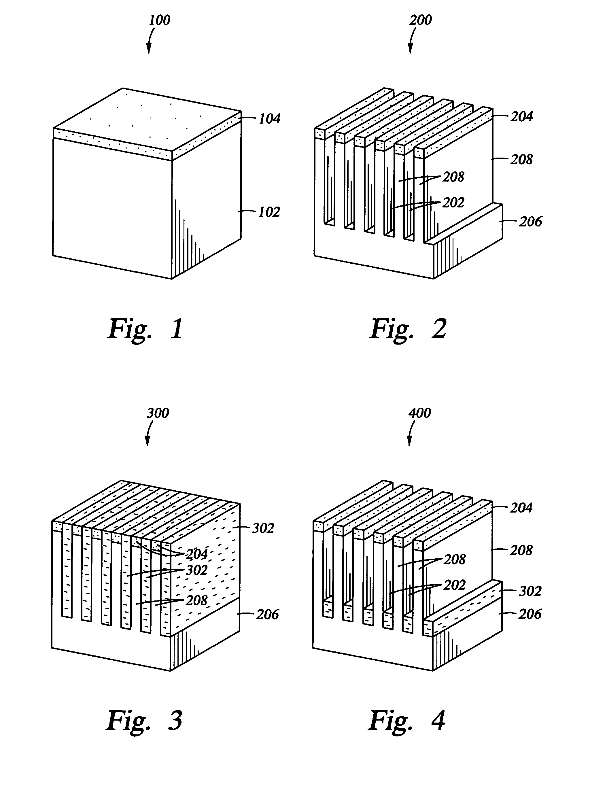
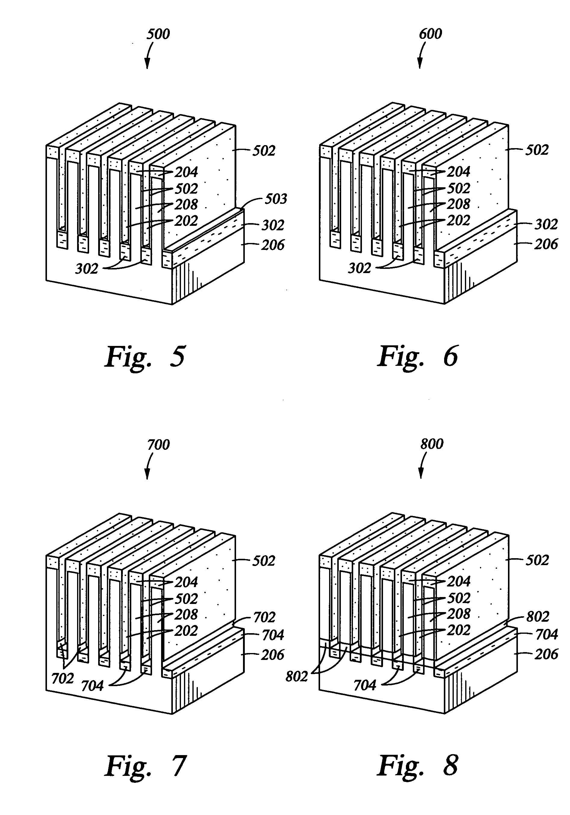
[0009]For a DRAM cell array, vertical channel transistors can provide area scaling advantage of about 33%. In the past, all contacts for the overall matrix of cells were made from the top of the array and this required additional space. A buried bit line (BBL) with sidewall connections on the exterior surfaces of the cell array is key to provide the most efficient production and functionality for vertical channel transistors for DRAM applications. To be able to use such outside sidewall connections for a cell array, there must be low line resistance along the bit lines. We use a self-aligning process flow to fabricate the BBL with low resistivity, this reduces processing costs and is advantageous for future scaling of banks of DRAM cells.

Problems solved by technology

In the past, all contacts for the overall matrix of cells were made from the top of the array and this required additional space.

Method used


Image

  • Method of fabricating a gate-all-around word line for a vertical channel DRAM
  • Method of fabricating a gate-all-around word line for a vertical channel DRAM
  • Method of fabricating a gate-all-around word line for a vertical channel DRAM

Examples


Embodiment Construction

[0059]As a preface to the detailed description, it should be noted that, as used in this specification and the appended claims, the singular forms “a”, “an”, and “the” include plural referents, unless the context clearly dictates otherwise.

[0060]When the word “about” is used herein, this is intended to mean that the nominal value presented is precise within ±10%.

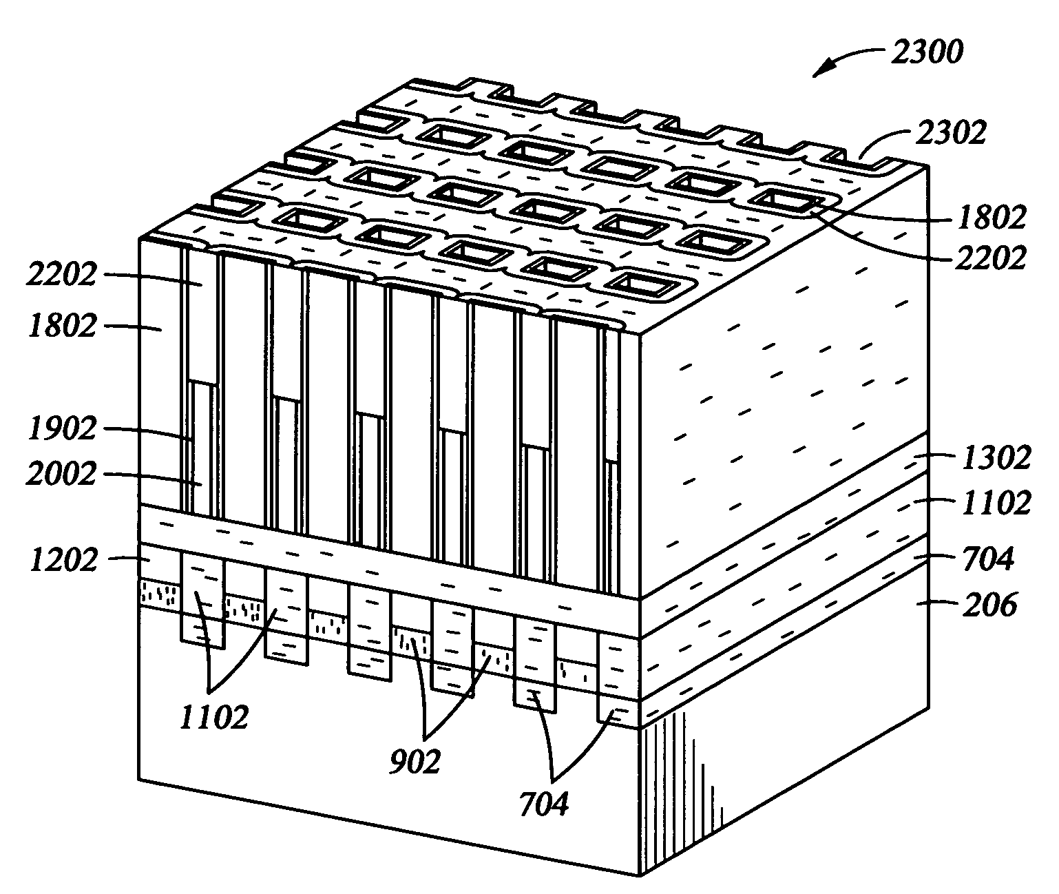
[0061]The present invention relates to an overall matrix for the location of individually-addressable DRAM cells and to a method of creating a buried wordline within that overall matrix. The present invention structure is described with reference to a related invention, which pertains to fabrication of a buried bit line. That structure is further processed to create a completed DRAM device structure, including a plurality of buried bit lines with accompanying electrically isolated buried wordlines, where an exterior upper surface of the structure is ready for capacitor application to each individually addressable DRAM cell. ...


PUM


Abstract

A method of fabricating a self-aligned buried wordline in a structure which contains a self-aligned buried bit line, where the overall structure which makes up a portion of a vertical channel DRAM. The materials and processes used enable self-alignment of elements of the buried wordline during the fabrication process. In addition, the materials and processes used enable for formation of individual DRAM cells which have a buried bit line width which is 16 nm or less and a perpendicular buried wordline width which is 24 nm or less.

Description

BACKGROUND OF THE INVENTION[0001]1. Technology Field[0002]The present application is related to a particularly compact structure comprising a plurality of vertical channel DRAM cells, with each cell having a self-aligned buried bit line and a gate-all-around word line, and to a method of fabricating this compact structure. The present application was filed simultaneously with a related application which relates to fabrication of a self-aligned buried bit line for a vertical channel DRAM. The related application number is 61 / 689,266, filed on May 31, 2012 and is entitled: “Method Of Fabricating A Self-Aligned Buried Bit Line For A Vertical Channel DRAM”. This related application is hereby incorporated by reference in its entirety.[0003]2. Description of the Background[0004]This section describes background subject matter related to the disclosed embodiments of the present invention. There is no intention, either express or implied, that the background art discussed in this section le...

Claims


Application Information

Patent Timeline
Patent Type & Authority Patents(United States)
IPC IPC(8): H01L27/108
CPCH01L27/10844H01L27/10891H01L27/10885H10B12/488H10B12/482H10B12/01
Inventor CHANG, CHORNG-PINGPING, ER-XUANPAN, JUDON TONY
Owner APPLIED MATERIALS INC
Why Eureka
Eureka Blog
Learn More