High intensity discharge electronic ballast circuit, electronic ballast, and high intensity discharge lamp

a high-intensity discharge and electronic ballast technology, applied in the field of electromechanical devices, can solve the problems of failure of electro magnetic compatibility test, and achieve the effects of improving luminous efficiency, low temperature and stable status, and efficient preventing stroboscopic

Inactive Publication Date: 2015-06-30
GUANGDONG GREENLIGHT PHOTOELECTRIC TECH
View PDF3 Cites 0 Cited by
  • Summary
  • Abstract
  • Description
  • Claims
  • Application Information

AI Technical Summary

Benefits of technology

[0015]Accordingly, an objective of the present invention is to provide an HID electronic ballast circuit, to improve luminous efficiency, and prevent stroboscopic effect generated in the electronic ballast circuit and solve problem of failed EMC test.
[0021]In the embodiments of the present invention, oscillation signals with a frequency range beyond “acoustics resonance” are generated by utilizing self-feedback of the inherent phase relationship of the power MOSFET, which efficiently prevents the stroboscopic effect and improves the luminous efficiency, and keeps the power MOSFET in a low-temperature and stable status and with high power. Furthermore, impedance matching for the oscillation signals is performed by the filter loop, thereby extending the frequency bandwidth and reducing the Q-value, and keeping the constant power supply at the same time, which makes the EMC test pass easily and improves the stability and reliability of the power output circuit. Additionally, the filter loop can replace a drive circuit to trigger the HID lamp, which simplifies the circuit and reduces the manufacturing cost.

Problems solved by technology

And a lot of higher harmonics may be generated during the square wave pulses supplying power, which causes electro magnetic compatibility (EMC) test failed.

Method used


Image

  • High intensity discharge electronic ballast circuit, electronic ballast, and high intensity discharge lamp
  • High intensity discharge electronic ballast circuit, electronic ballast, and high intensity discharge lamp
  • High intensity discharge electronic ballast circuit, electronic ballast, and high intensity discharge lamp

Examples


Embodiment Construction

[0028]Other aspects, features, and advantages of this invention will become apparent from the following detailed description when taken in conjunction with the accompanying drawings, which are a part of this disclosure and which illustrate, by way of example, principles of this invention.

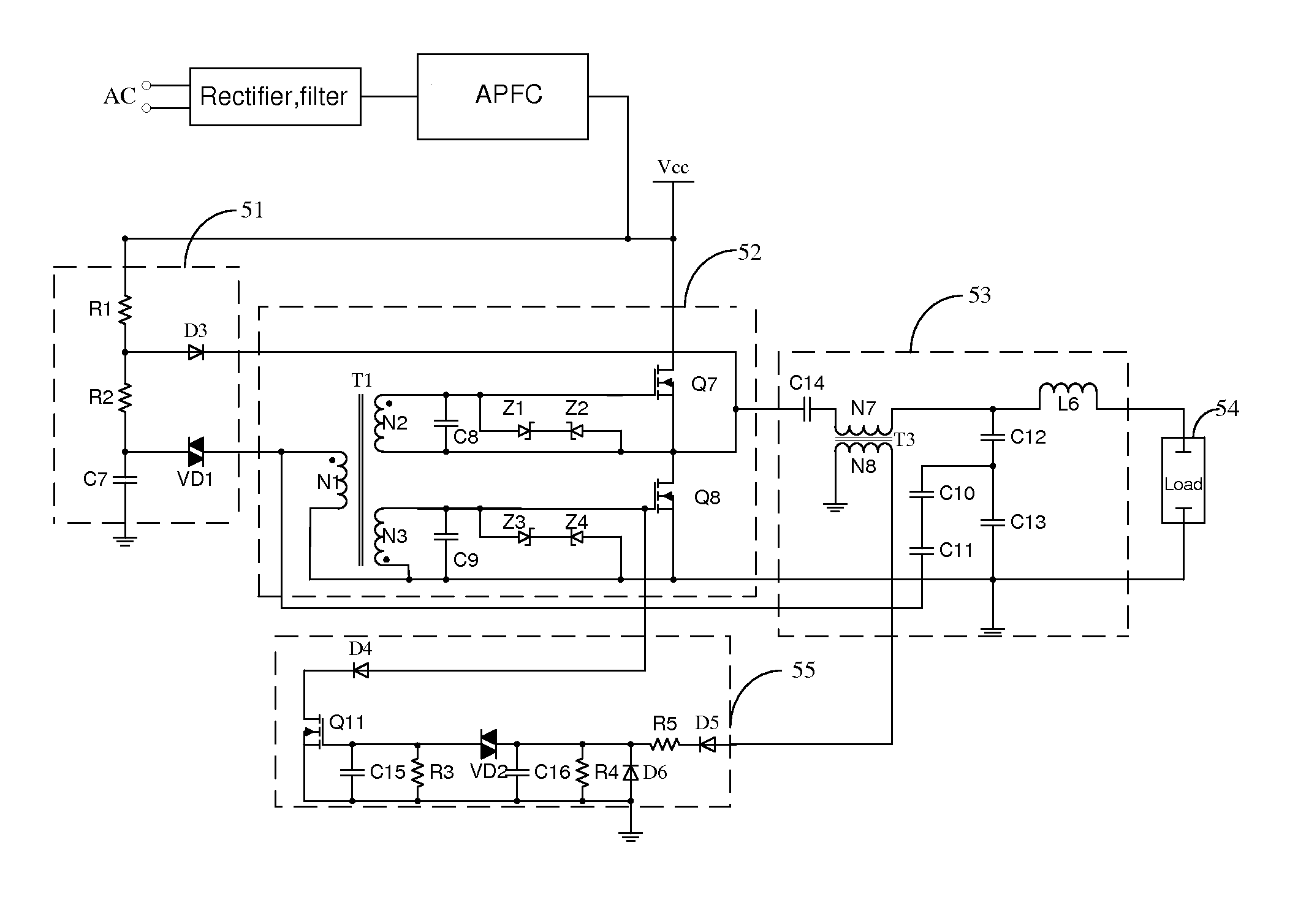
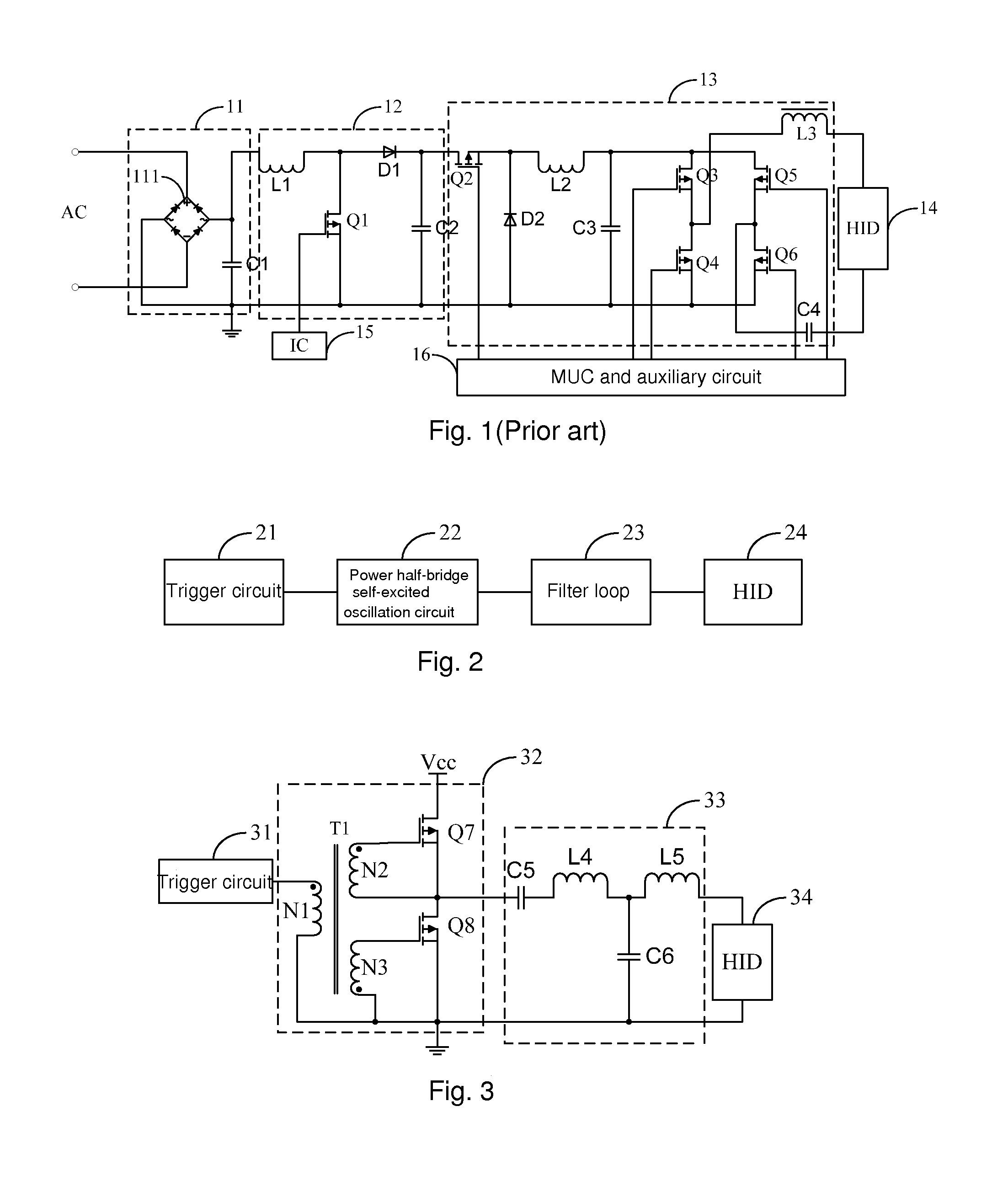
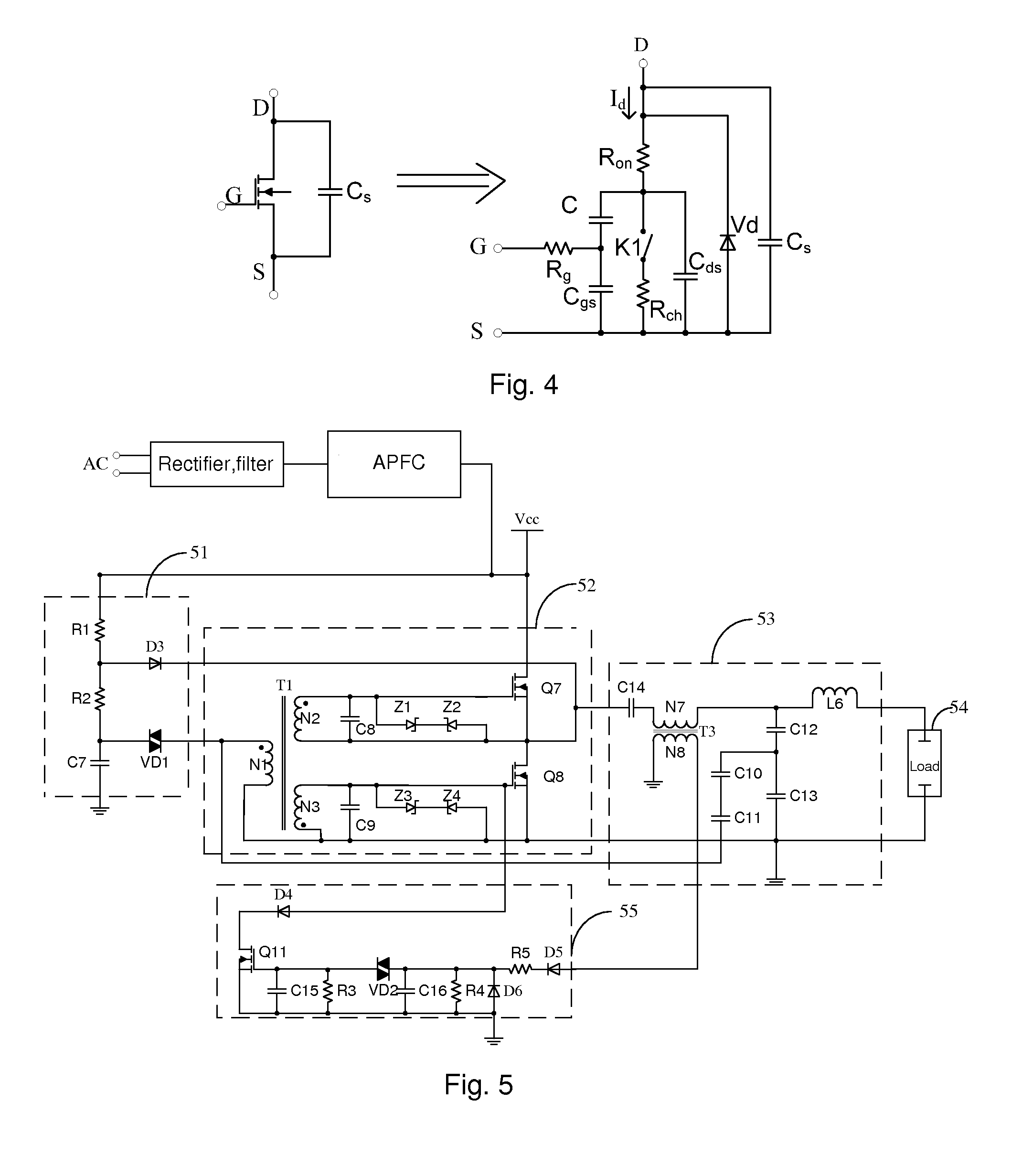
[0029]With the embodiments of the present invention, the inherent phase relationship of the power MOSFET (Metallic Oxide Semiconductor Field Effect Transistor) is utilized, and oscillation signals are generated by a power half-bridge self-excited oscillation circuit, and then impedance matching for the oscillation signals is performed by a filter loop, and finally an HID lamp is triggered. As a result, damages to human eyes caused by stroboscopic effect can be avoided and electro magnetic compatibility (EMC) test can be passed.

[0030]FIG. 2 is a structural diagram of an HID electronic ballast circuit according to an embodiment of the present invention. For convenience to explain, only relevant parts ...


PUM


Abstract

A high intensity discharge (HID) ballast circuit comprises a trigger circuit, a power half-bridge self-excited oscillation circuit, which is arranged to enable self-excited oscillation by energizing an angle capacitor Cgs with a Miller capacitor Cdg of a power MOSFET when an original single pulse output by the trigger circuit is excited, and then output self-excited oscillation signals; and a filter loop which is arranged to match impedance for the self-excited oscillation signals, thereby converting a low-impedance voltage source to a high-impedance constant current source. The inherent phase relationship of the power MOSFET is utilized, and oscillation signals are generated by a power half-bridge self-excited oscillation circuit, and then impedance matching for the oscillation signals is performed by the filter loop, and finally an HID lamp is triggered. As a result, damages to human eyes caused by stroboscopic effect can be avoided and electro magnetic compatibility test can be passed.

Description

FIELD OF THE INVENTION[0001]The present invention relates to an electronic technical field, and more particularly to a high intensity discharge electronic ballast circuit, an electronic ballast, and a high intensity discharge lamp.BACKGROUND OF THE INVENTION[0002]As an increasing demand of the energy saving lighting in the current society, high intensity discharge (HID) lamps have replaced halogen lampa and high-tension mercury lamps and become a new efficient light source in the world due to their advantages such as energy saving and high light, etc. While a ballast in the HID lamp is the most important part that determines the quality of the HID lamp.[0003]Generally, the HID ballasts include HID electronic ballasts and HID inductive ballasts. And the HID ballasts has replaced the HID inductive ballasts due to their outstanding advantages, such as a constant power, less power pollution, high utilization of power, and efficient photoelectric conversion.[0004]FIG. 1 illustrates a sch...

Claims


Application Information

Patent Timeline
Patent Type & Authority Patents(United States)
IPC IPC(8): H05B41/00H05B37/02H05B39/02H05B39/04H05B41/16H05B41/288
CPCH05B41/16H05B41/2882
Inventor XIE, LISHANCHEN, YUJIAYUAN, QINGHUIYANG, HONGMIN
Owner GUANGDONG GREENLIGHT PHOTOELECTRIC TECH
Why Eureka
Try Eureka