
Power amplifier with co-existence filter

a technology of power amplifier and filter, which is applied in the field of radio frequency signal circuitry, can solve the problems of increasing the overall footprint of the printed circuit board, spurious noise and interference, and the insufficient power of conventional mobile handset transceivers, and achieves the effect of minimizing the instability of the filter

Active Publication Date: 2015-07-28
SKYWORKS SOLUTIONS INC
View PDF31 Cites 9 Cited by
  • Summary
  • Abstract
  • Description
  • Claims
  • Application Information

AI Technical Summary

Benefits of technology

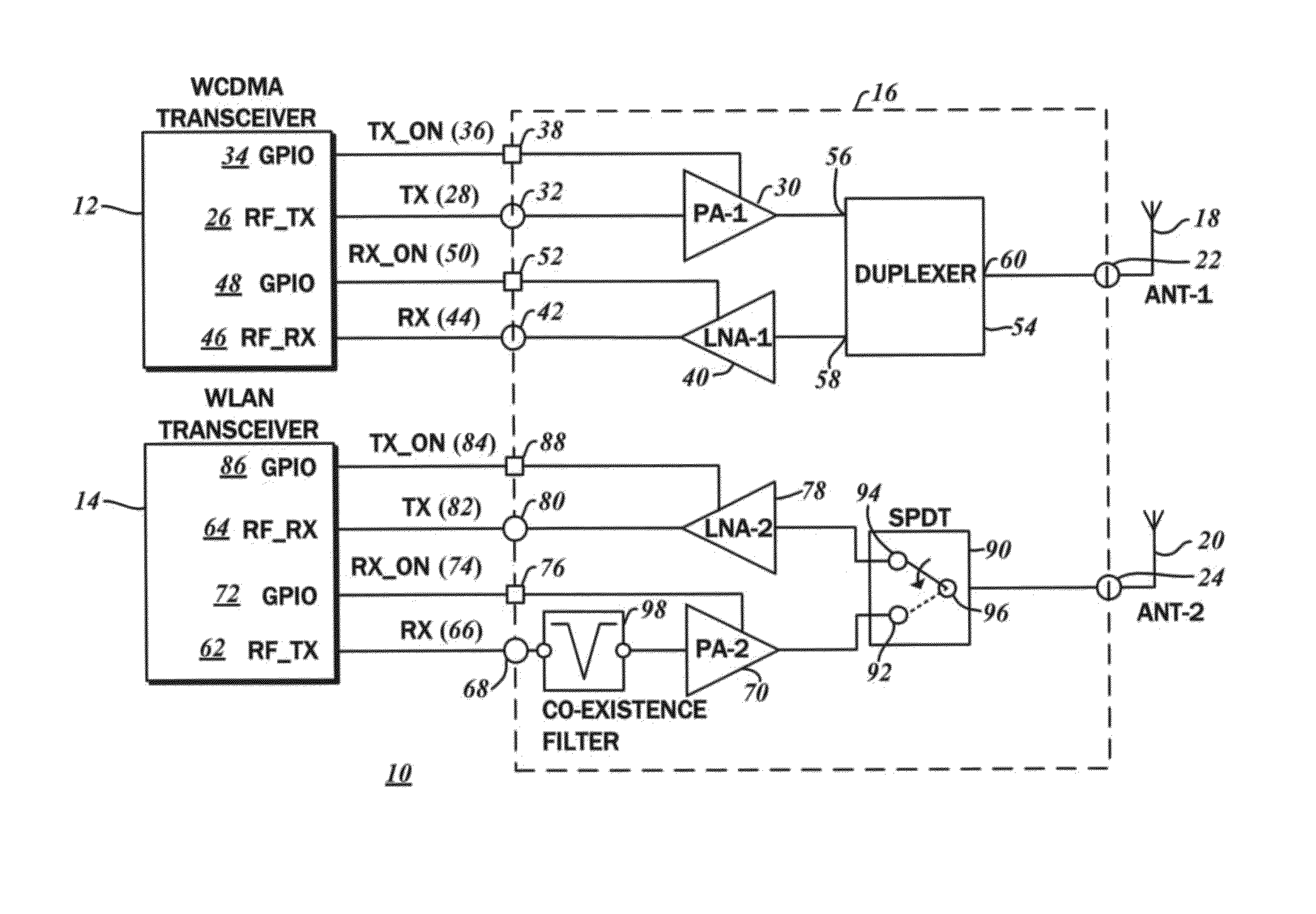
[0013]In accordance with various embodiments of the present disclosure, there is contemplated a power amplifier architecture for connecting a transceiver to an antenna, and include an input port and an output port. The transceiver may be configured for a specific operating frequency. There may be an input matching segment that connected to the input port, as well as an output matching segment that is connected to the output port. There may be at least one filter with a range of rejection frequencies. The power amplifier architecture may also include an amplifier segment that may have at least one transistor with a first terminal connected to the input matching segment, a second terminal connected to the output matching segment, and a third terminal connected to the filter. The filter may be connected in close proximity to a first inductive interconnection tying a junction connected to the third terminal to a ground. Furthermore, there may be a compensator that is connected to the input matching segment and the output matching segment to minimize instability of the filter.

Problems solved by technology

Conventional mobile handset transceivers typically do not generate sufficient power or have sufficient sensitivity for reliable communications standing alone.
There are a number of challenges associated with this, one of these being the crowded RF environment within which the WLAN subsystem operates.
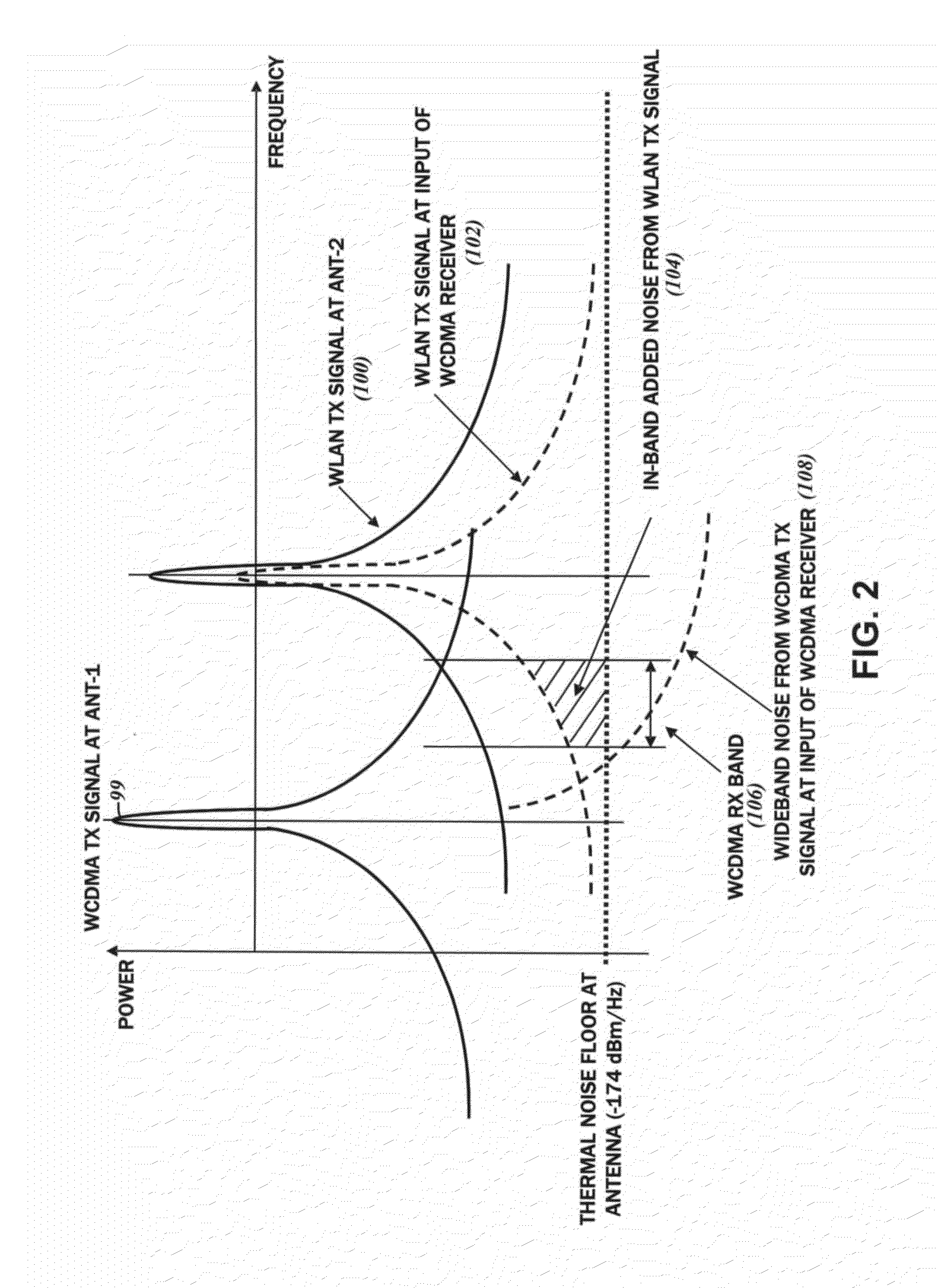
The transmissions from the WLAN subsystem, notwithstanding different operating frequencies, tend to cause spurious noise and interference.
The diminutive size of the handset and the attendant necessity for positioning the respective antennas of the different communications subsystems in relatively close proximity to each other add another layer of challenges.
However, these are typically low temperature co-fired ceramic (LTCC) devices that tend to be bulkier and thereby increase the overall footprint of the printed circuit board.
Furthermore, such co-existence filters also degrade the performance of the WLAN system due to increased current consumption and degraded reception sensitivity.
The fabrication of such filters can be accomplished with a smaller footprint, but the costs are significantly higher.
The filter is typically connected at the input of the power amplifier, and though it would be advantageous to fabricate the same on-die, the performance of such implementations is inadequate.
Problematically, the fairly low Q-factors of on-die components necessitated the addition of an external co-existence filter.
This would require a higher output from the power amplifier, thereby leading to greater current consumption from the power source (battery).
The insertion loss associated with the external co-existence filter also decreases the receive sensitivity of the WLAN chain, adversely affecting the link distance and data throughput.

Method used


Image

  • Power amplifier with co-existence filter
  • Power amplifier with co-existence filter
  • Power amplifier with co-existence filter

Examples


first embodiment

[0064]With reference to the schematic diagram of FIG. 4, the co-existence filter 98a includes a capacitor C2 connected to a junction 128 that is tied to a third terminal 116c of the transistor 116. Connected in series with the capacitor C2 is an inductor L2 tied to ground. As indicated above, there is an inductance 122 that corresponds to the bond wire that ties the third terminal 116c to ground, and this is shown as inductor L1. Similarly, the inductor L2 is also implemented as a bond wire with a high Q-factor. The bond wires corresponding to the inductors L1 and L2 are positioned in close proximity to each other, and the coupling coefficient between the die pads for the bond wires define a coupling coefficient which has typical values of 0.4 to 0.5.

[0065]The values for the capacitor C2 and the inductors L2 and L1 are selected such that the impedance at junction 116c looking from emitter side down at the WLAN operating frequency (2.4 GHz to 2.5 GHz), there is a small resistive valu...

second embodiment

[0067]Referring now to the schematic diagram of FIG. 6, there is depicted the co-existence filter 98b. This variation likewise includes the capacitor C2 connected to the junction 128 tied to the third terminal 116c, and the inductor L2 connected in series with the capacitor C2 and tied to ground. Additionally, there is a capacitor C3 also connected to the junction 128, and an inductor L3 connected in series with the capacitor C3 and tied to ground. As indicated above, the inductor L1 may implemented as a bond wire that ties the third terminal 116c of the transistor 116 to ground. Along these lines, the inductors L2 and L3 may also be bond wires that are physically positioned in close proximity to each other. The coupling coefficient between the die pads of the inductor L1 and the inductor L2, as well as between those of the inductor L1 and the inductor L3 are understood to be typically 0.4 to 0.5, while the coupling coefficient between die pads of the inductor L2 and the inductor L3...

third embodiment

[0069]The schematic diagram of FIG. 8 illustrates yet another, third embodiment of the co-existence filter 98c. In this embodiment, an inductor L4 separates the junction 128 from the third terminal 116c of the transistor 116. However, the capacitor C3 in series with the inductor L3 is directly connected to the third terminal 116c, while the second capacitor C2 in series with the second inductor L2 remains connected to the junction 128. Again, each of the inductors L1, L2, and L3 are implemented as bond wires, and the die pads to which they are attached define various magnetic coupling coefficients that are in line with the parameters discussed above.

[0070]The various components of the co-existence filter 98c can be adjusted to exhibit the aforementioned impedance characteristics at the operating frequency and the rejection frequency band, and the simulated response shown in the Smith chart of FIG. 9 illustrates conformance therewith. The third embodiment of the co-existence filter 9...


PUM


Abstract

A power amplifier architecture and front end circuits utilizing the same that connect a transceiver to an antenna are disclosed. The transceiver is configured for a specific operating frequency. An input matching segment is connected to an input port, and an output matching segment is connected to an output port. An amplifier segment includes at least one transistor with a first terminal connected to the input matching segment, a second terminal connected to the output matching segment, and a third terminal connected to a filter with a range of rejection frequencies. The filter is connected in close proximity to a first inductive interconnection tying a junction connected to the third terminal to a ground. A compensator is also connected to the input matching segment and the output matching segment to minimize instability of the filter.

Description

CROSS-REFERENCE TO RELATED APPLICATIONS[0001]This application relates to and claims the benefit of U.S. Provisional Application No. 61 / 481,557, filed May 2, 2011 and entitled WLAN POWER AMPLIFIER ARCHITECTURE WITH CO-EXISTENCE FILTER FOR WCDMA HANDSET APPLICATIONS, which is wholly incorporated by reference herein.STATEMENT RE: FEDERALLY SPONSORED RESEARCH / DEVELOPMENT[0002]Not ApplicableBACKGROUND[0003]1. Technical Field[0004]The present disclosure relates generally to radio frequency (RF) signal circuitry, and more particularly, to wireless local area network (WLAN) power amplifiers with a co-existence filter for mobile wireless communications devices.[0005]2. Related Art[0006]Wireless communications systems find application in numerous contexts involving data transfer over long and short distances alike, and there exists a wide range of modalities suited to meet the particular needs of each. Chief amongst these systems with respect to popularity and deployment is the mobile or cell...

Claims


Application Information

Patent Timeline
Patent Type & Authority Patents(United States)
IPC IPC(8): H04B1/38H03H7/01H03F3/72H03F3/195H03F3/24H03F1/56H03F3/68
CPCH03F3/68H03F1/565H03F3/195H03F3/24H03F3/72H03H7/1741H03F2200/222H03F2200/294H03F2200/387H03F2200/117H03F2200/138H03F2200/147H03F2200/489H03F2200/492H03F2200/501
Inventor GORBACHOV, OLEKSANDR
Owner SKYWORKS SOLUTIONS INC
Learn More