
Touch panel, display panel, and display unit

a display panel and touch panel technology, applied in the field of touch panel, display panel, display unit, can solve the problems of erroneous detection, touch of a finger is erroneously detected, surface electric field change of the panel, etc., to eliminate external noise from detection signals, high sensitivity to contact/noncontact state, effect of low sensitivity

Active Publication Date: 2015-09-01
JAPAN DISPLAY INC
View PDF5 Cites 8 Cited by
  • Summary
  • Abstract
  • Description
  • Claims
  • Application Information

AI Technical Summary

Benefits of technology

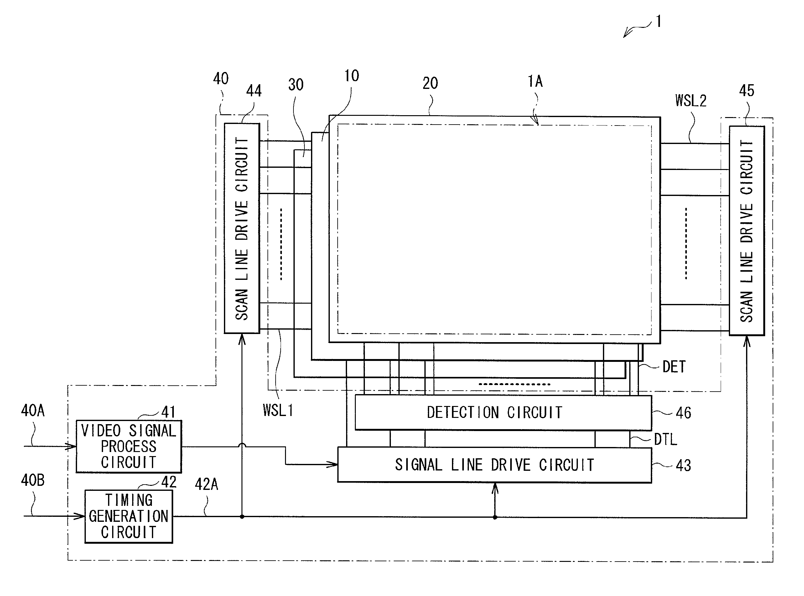
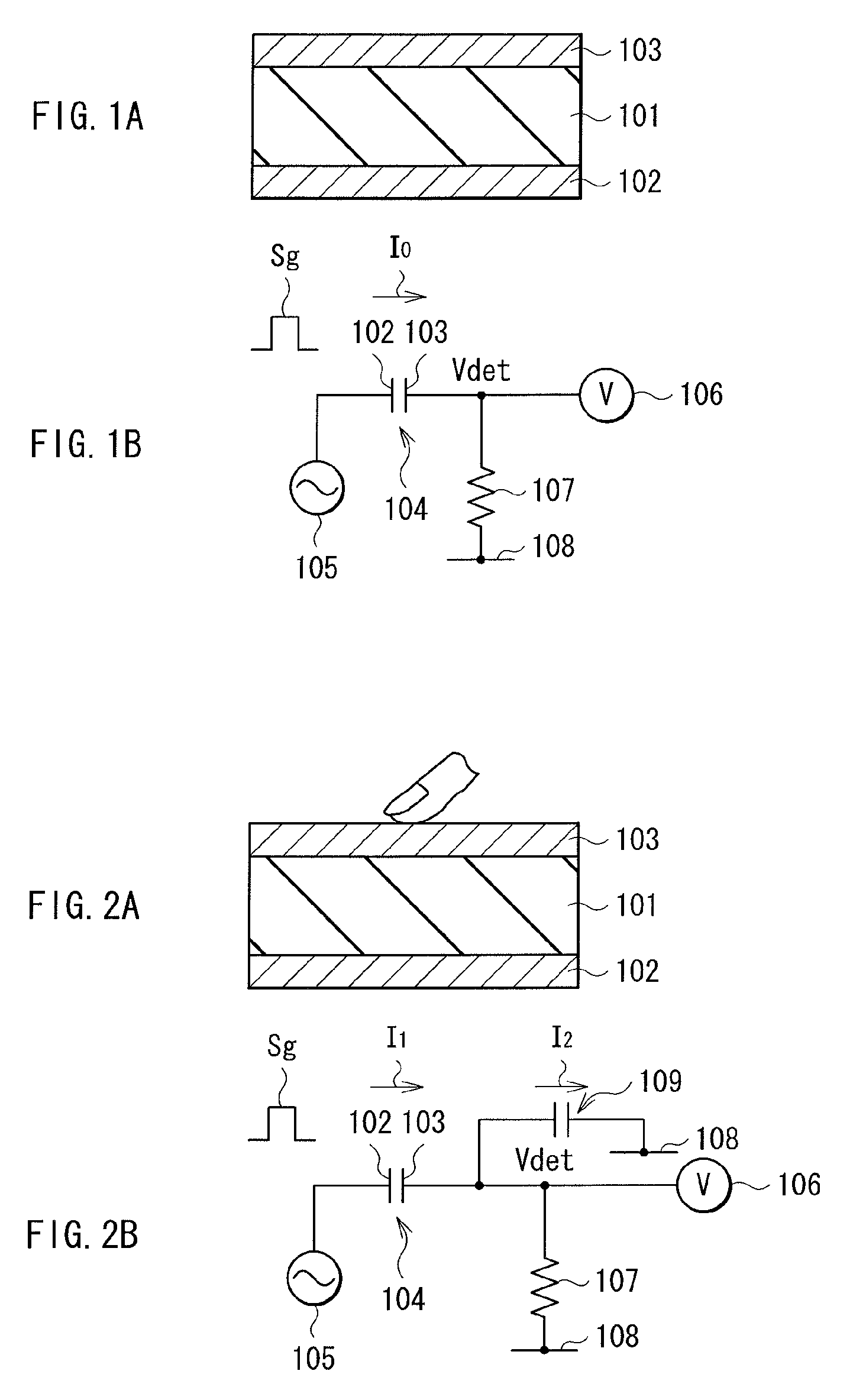
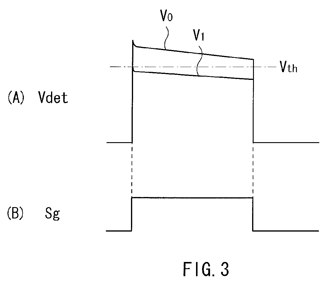
The present invention provides a touch panel, display panels, and display units that can eliminate erroneous detection caused by external noise. This is achieved by providing at least two kinds of detection electrodes with different sensitivities to the contact / noncontact state. By obtaining the difference between the detection signals obtained from these electrodes, external noise is eliminated from the detection signals. This allows for more accurate detection of external objects touching the touch panel.

Problems solved by technology

Consequently, in the case where noise from the outside enters the capacitive element, the surface electric field of the panel changes due to the noise, and there is a possibility that touch of a finger is erroneously detected.
In particular, in the case where the user of a display device plays the role of an antenna and catches external noise, there is a problem such that when the user touches the panel with a finger or the like, the external noise is transmitted via the finger or the like to the panel, the surface electric field of the panel changes, and it causes erroneous detection.

Method used


Image

  • Touch panel, display panel, and display unit
  • Touch panel, display panel, and display unit
  • Touch panel, display panel, and display unit

Examples


first embodiment

Modification of First Embodiment

[Modification 1]

[0144]Although the case where one scan electrode 22 is connected to one scan line WSL2 has been described in the foregoing embodiment, the plurality of neighboring scan electrodes 22 may be connected to one scan line WSL2. In such a case, as compared with the case where one scan electrode 22 is connected to one scan line WSL2, the signal level of the detection signal Vdet obtained from the detection electrodes 25 and 26 becomes higher. Incidentally, only by simply increasing the line width of the scan electrode 22 and the detection electrodes 25 and 26, the signal level of the detection signal Vdet is made higher. However, in such a case, as described above, when the line width is increased, only the parallel plate capacitance C1 increases, and the capacitance C and the capacitance D decrease. Therefore, the sensitivity to touch with a finger or the like decreases. On the other hand, as in the present modification, in the case of conne...

second embodiment

Modification of Second Embodiment

[Modification 1]

[0168]Although the case where one scan electrode 22 is connected to one scan line WSL2 has been described in the foregoing embodiment, the plurality of neighboring scan electrodes 22 may be connected to one scan line WSL2. In such a case, as compared with the case where one scan electrode 22 is connected to one scan line WSL2, the signal level of the detection signal Vdet obtained from the detection electrodes 27 and 28 is made higher.

[Modification 2]

[0169]In the foregoing embodiment, the detection electrodes 27 and 28 are formed so that the capacitances C and D become almost equal to each other. However, for example, due to manufacture error or the like, there may be a case that the capacitances C and D are slightly different from each other. On the assumption of such a case, for example, the output adjustment circuit 56 as shown in FIG. 16 may be further provided as means for ensuring that the erroneous detection caused by the exter...

third embodiment

[0170]FIG. 19 illustrates an example of the top face configuration of the touch panel 20 included in a liquid crystal display device according to a third embodiment of the invention. The liquid crystal display device of the third embodiment is different from the liquid crystal display device 1 of the foregoing embodiment, in that a plurality of detection electrodes 29 are provided in place of the plurality of detection electrodes 25 and 26, and a plurality of detection electrodes 31 are provided in place of the plurality of detection electrodes 22 in the touch panel 20. In the following, the points different from the configuration of the foregoing embodiment will be mainly described, and description of the configuration common to that of the foregoing embodiment will not be repeated.

[0171]In the present embodiment, as one of electrodes in the touch sensor of the electrostatic capacitance type, only one kind of the detection electrode 29 is provided. That is, different from the first...


PUM


Abstract

A touch panel, a display panel, and a display unit achieving prevention of erroneous detection caused by external noise, are provided. The touch panel includes: a plurality of detection scan electrodes extending in a first direction; and a plurality of detection electrodes facing the plurality of detection scan electrodes and extending in a second direction which intersects the first direction. A ratio of fringe capacitance to total capacitance between one or more selected detection scan electrodes and a first detection electrode is different from a ratio of fringe capacitance to total capacitance between the one or more selected detection scan electrodes and a second detection electrode. The one or more selected detection scan electrodes are selected, in a desired unit, from the plurality of detection scan electrodes, to be supplied with a selection pulse, and each of the first and the second detection electrodes is selected from the plurality of detection electrodes.

Description

BACKGROUND OF THE INVENTION[0001]1. Field of the Invention[0002]The present invention relates to a touch panel, a display panel, and a display unit enabling information to be entered by being touched with an object such as a finger or pen.[0003]2. Description of the Related Art[0004]Techniques of entering information by touch with a finger or the like are known. Among them, a technique attracting particular attention is a display device capable of entering information by touching various buttons displayed on a display with a finger or the like in a manner similar to the case of touching normal buttons with a finger or the like. The technique allows the display and the buttons to be commonly used and therefore brings large advantages of smaller space and reduction in the number of parts.[0005]Various types of touch sensors that detect a touch of a finger or the like exist. A popularized touch sensor is, for example, of an electrostatic capacitance type. A touch sensor of this type ca...

Claims


Application Information

Patent Timeline
Patent Type & Authority Patents(United States)
IPC IPC(8): G06F3/045G06F3/047H01J11/12G06F3/0354G09G3/298G06F3/044
CPCG06F3/044G06F3/03547G06F3/047G09G3/2983G09G3/2986H01J11/12G06F3/0446G06F3/0418G06F3/0445G02F1/134363G06F3/0448G02F1/134372G06F3/0412G09G3/3696G09G2330/06
Inventor NAKANISHI, TAKAYUKINOGUCHI, KOJIISHIZAKI, KOJITERANISHI, YASUYUKITAKEUCHI, TAKEYA
Owner JAPAN DISPLAY INC
Learn More