Miniaturize voltage-transforming device

a voltage-transforming device and miniature technology, applied in the direction of process and machine control, electronic circuit device association, printed circuit non-printed electric components, etc., can solve the problems that the existing electronic circuit device does not meet the trend toward miniaturization and compactness, and achieve the effect of reducing the overall volume of the whole assembly

Active Publication Date: 2015-09-29
POWER MATE TECH CO LTD
View PDF7 Cites 5 Cited by
  • Summary
  • Abstract
  • Description
  • Claims
  • Application Information

AI Technical Summary

Benefits of technology

[0006]The primary objective of the present invention is to provide a miniaturized voltage-transforming device, which integrates its circuit boards and transformer into a three-dimensional structure, thereby reducing the overall volume of the whole assembly, thereby achieving miniaturization.

Problems solved by technology

In view of this, the existing electronic circuit devices are not satisfying the trend toward miniaturization and compactness in the field of electronic products and need to be improved.

Method used


Image

  • Miniaturize voltage-transforming device
  • Miniaturize voltage-transforming device
  • Miniaturize voltage-transforming device

Examples


first embodiment

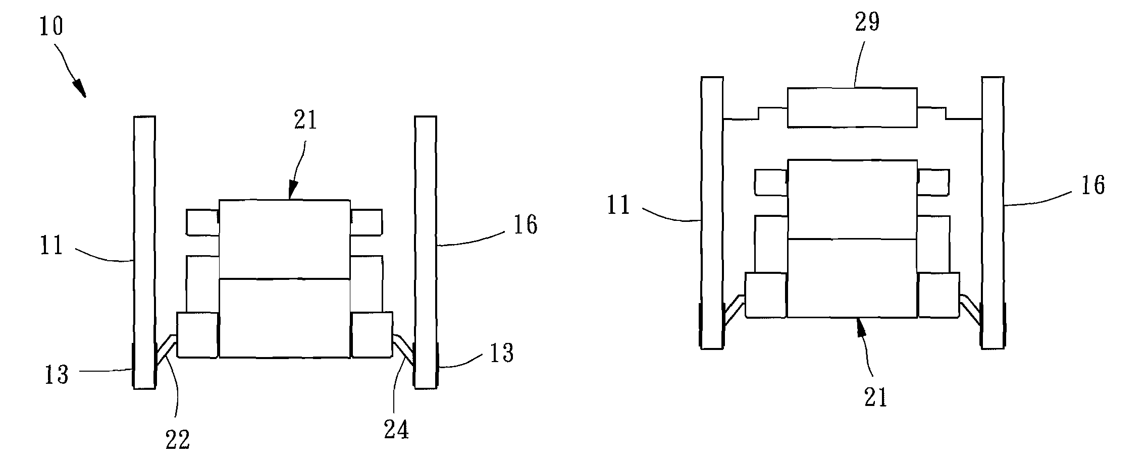
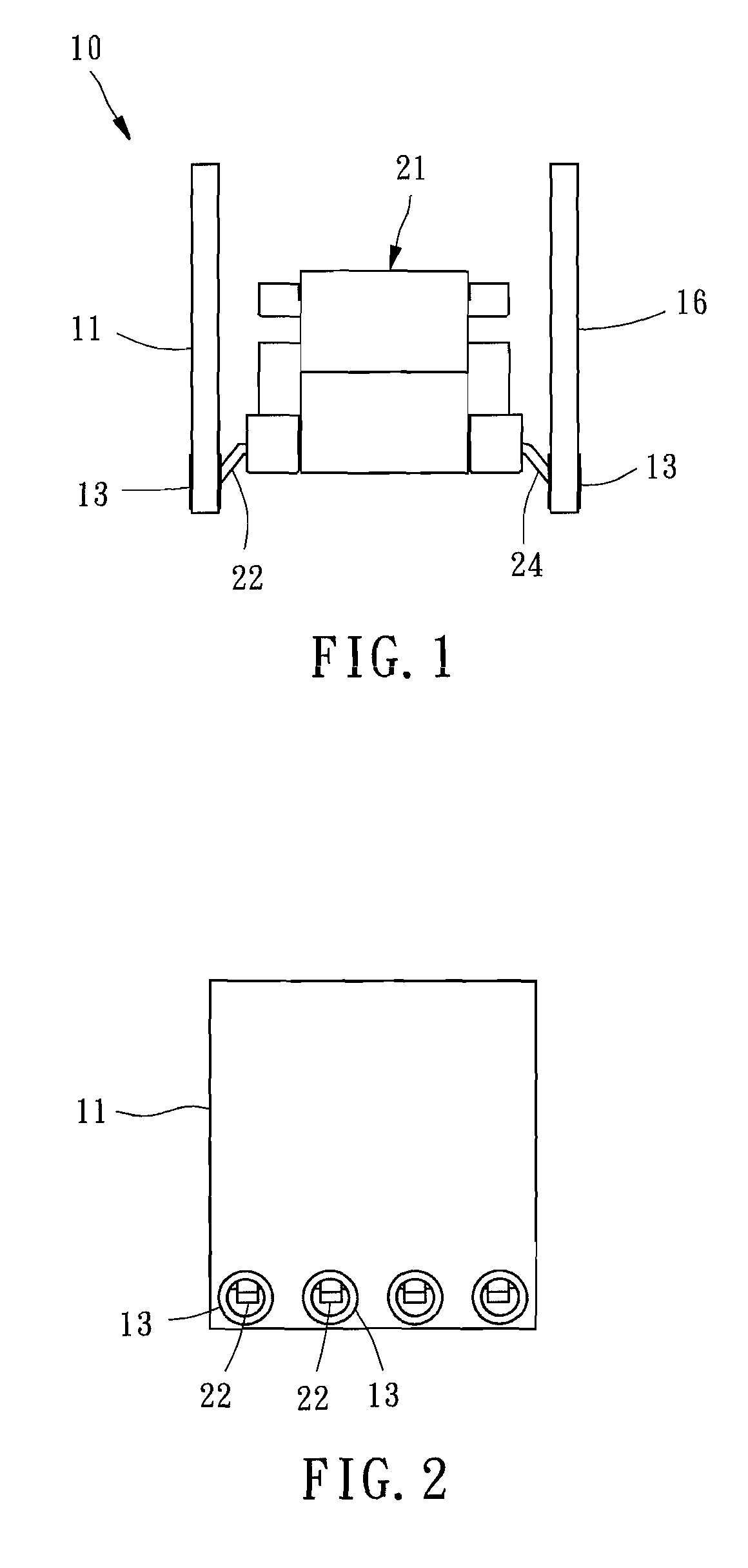
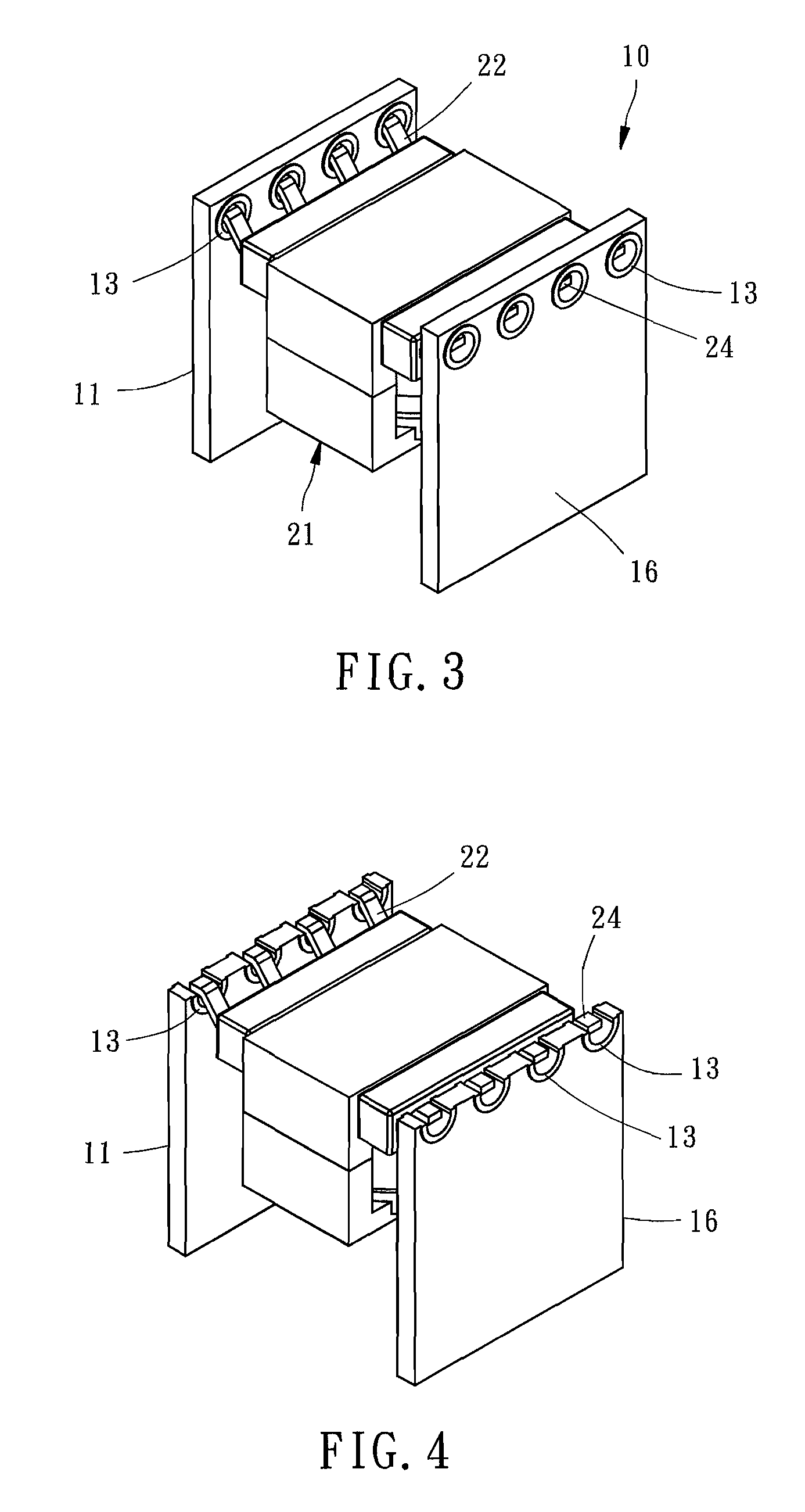
[0031]In the first embodiment, the primary-side pins 22 and the secondary-side pins 24 are located at two laterals of the transformer 21, respectively. The first circuit board 11 and the second circuit board 16 are deposited beside the two laterals of the transformer 21, so that the primary-side pins 22 are at the same side of the first circuit board 11 and are physically connected to the first circuit board 11, while the secondary-side pins 24 are at the same side of the second circuit board 16 and are physically connected to the second circuit board 16. Thereby the primary-side pins 22 and the secondary-side pins 24 are directly connected to the first circuit board 11 and the second circuit board 16, respectively. The transformer 21 is between facing surfaces of the first circuit board 11 and the second circuit board 16, making it look like sandwiched by the first and second circuit boards 11 and 16.

[0032]Additionally, in the first embodiment, the first circuit board 11 has a plur...

second embodiment

[0038]The miniaturized voltage-transforming device 30 of the second embodiment further has a third circuit board 37 and a flexible circuit board 39. The flexible circuit board 39 is physically mounted on the first circuit board 31, the third circuit board 37 and the second circuit board 36, and is electrically connected to the first circuit board 31 and the second circuit board 36, or may be further electrically connected to the third circuit board 37 as needed. The first circuit board 31, the second circuit board 36 and the third circuit board 37 are not physically connected to each other, but each two adjacent said circuit boards are mutually pivotable about a connection therebetween caused by the flexible circuit board 39.

[0039]The transformer 41 is deposited on the third circuit board 37 and between the first circuit board 31 and the second circuit board 36. The primary-side pins 42 and the secondary-side pins 44 are physically connected to the flexible circuit board 39, and in ...

third embodiment

[0045]Thereby, the third embodiment can also accomplish the desired three-dimensional structure of the first circuit board 51, the second circuit board 56 and the transformer 61, so the overall volume of the assembly is miniaturized.

[0046]The other details and effects of the third embodiment are similar to those of the first embodiment and no repeated description is provided herein.


PUM

PropertyMeasurementUnit
distanceaaaaaaaaaa
flexibleaaaaaaaaaa
conductiveaaaaaaaaaa

Abstract

A miniaturized voltage-transforming device includes a first circuit board and a second circuit board parallel to and separated from each other by a predetermined distance so that there is no physical connection therebetween, and a transformer having a plurality of primary-side pins and a plurality of secondary-side pins, wherein the transformer is located beside the first circuit board and the second circuit board, and has its primary-side pins and secondary-side pins directly or indirectly connected to the first circuit board and the second circuit board physically, so that the transformer is electrically connected to the first circuit board and the second circuit board via the primary-side pins and the secondary-side pins.

Description

BACKGROUND OF THE INVENTION[0001]1. Technical Field[0002]The present invention relates to structures of electronic circuit devices, and more particularly to a miniaturized voltage-transforming device.[0003]2. Description of Related Art[0004]A conventional electronic circuit device depicted in FIG. 11 is, for example, a transformer-based apparatus, which includes a transformer 91 that is deposited on a circuit board 96 and has primary-side and secondary-side pins 92, 93 directly welded on and electrically connected to the circuit board 96, thereby providing voltage-regulating function.[0005]In the foregoing conventional electronic circuit device, the circuit board is merely a planar board, so it can only receive other electronic components with its, at most, upper and lower surfaces. The only way to enlarge the available installation space for additional electronic components is to enlarge the circuit board itself, leading to the increased overall volume of the whole assembly. In vie...

Claims


Application Information

Patent Timeline
Patent Type & Authority Patents(United States)
IPC IPC(8): H01F5/00H05K1/14H01F27/29H02M7/00H05K1/18H05K3/34H02M3/00H05K3/40H01F27/40
CPCH02M7/003H01F5/00H01F27/292H02M3/00H05K1/145H05K1/18H05K1/189H05K3/3405H01F27/402H01F2027/297H05K1/144H05K1/148H05K3/3447H05K3/403H05K2201/042H05K2201/047H05K2201/09181H05K2201/1003H02M3/003
Inventor CHEN, LIEN-HSINGLIU, LI-HAOTSAI, CHENG-TE
Owner POWER MATE TECH CO LTD
Why Eureka
Try Eureka