A method of manufacturing a pcb

A manufacturing method and substrate technology, applied in printed circuit manufacturing, multi-layer circuit manufacturing, crosstalk/noise/electromagnetic interference reduction (and other directions, can solve the problem that components with special-shaped structures cannot be mounted, and components cannot be realized at the same time. Special assembly requirements, single shape of the first step groove, etc., to save installation space, reduce assembly volume, and facilitate placement

Active Publication Date: 2019-11-29
DONGGUAN SHENGYI ELECTRONICS
View PDF8 Cites 0 Cited by
  • Summary
  • Abstract
  • Description
  • Claims
  • Application Information

AI Technical Summary

Problems solved by technology

[0004] 1) The shape of the first-order stepped groove is single, and it is impossible to mount components with special-shaped structures;
[0005] 2) A single metallized or non-metallized stepped groove cannot meet the special assembly requirements of components at the same time, or integrate other more power amplifier devices

Method used


Image

  • A method of manufacturing a pcb
  • A method of manufacturing a pcb
  • A method of manufacturing a pcb

Examples


Embodiment Construction

[0035] The technical solutions of the present invention will be further described below in conjunction with the accompanying drawings and through specific implementation methods. It should be understood that the specific embodiments described here are only used to explain the present invention, but not to limit the present invention. In addition, it should be noted that, for the convenience of description, only the parts related to the present invention are shown in the drawings but not all of them.

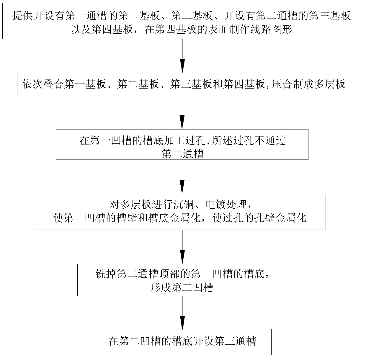
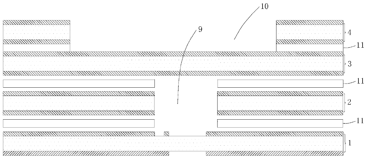
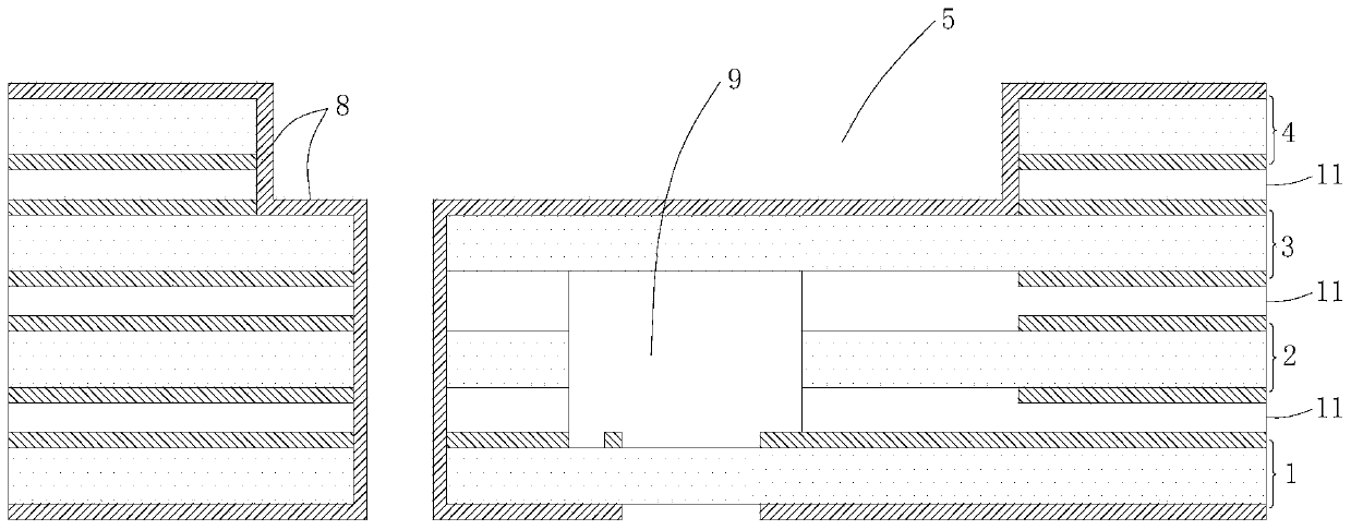
[0036] Such as figure 1 Shown, a kind of manufacturing method of PCB comprises the following steps:

[0037] Step 1. Provide the first substrate 4 with the first through groove 10, the second substrate 3, the third substrate 2 with the second through groove 9, and the fourth substrate 1, and fabricate on the surface of the fourth substrate 1. Line graphics.

[0038] The first substrate 4, the second substrate 3, the third substrate 2 and the fourth substrate 1 are respectively...


PUM


Abstract

The invention relates to the technical field of circuit board production, and discloses a manufacturing method of a PCB, comprising the following steps: S1, providing a first substrate having a firstthrough groove, a second substrate, a third substrate having a second through groove and a fourth substrate, and forming a circuit pattern on the surface of the fourth substrate; S2, sequentially laminating the first substrate, the second substrate, the third substrate and the fourth substrate, and forming a multilayer board by compression; S3, subjecting the multilayer board to copper immersion and electroplating to metallize the groove wall and the groove bottom of a first groove; S4, milling the groove bottom of the first groove at the top of the second through groove to form a second groove; and S5, forming a third through groove in the groove bottom of the second groove. The manufacturing method of the PCB according to the present invention realizes the mounting of the special-shapedcomponent and a plurality of components of different sizes, reduces the occupied space of the PCB, and forms a circuit pattern at the groove bottom of the stepped groove, which is beneficial to further miniaturization of the PCB.

Description

technical field [0001] The invention relates to the technical field of circuit board production, in particular to a method for manufacturing a PCB. Background technique [0002] Printed circuit board (PCB for short) is the provider of electrical connection for electronic components. Before the appearance of printed circuit boards, the interconnection between electronic components relied on the direct connection of wires to form a complete circuit. In contemporary times, circuit panels only exist as effective experimental tools, and printed circuit boards have occupied an absolute dominant position in the electronics industry. [0003] In order to meet the high-density mounting or crimping requirements of printed circuit boards, multi-layer printed circuit boards are designed to open stepped grooves to reduce the assembly volume. The current stepped groove design mostly shows first-order metallization or non-metallization Step slots are used in microwave radio frequency pro...

Claims


Application Information

Patent Timeline
Patent Type & Authority Patents(China)
IPC IPC(8): H05K3/46H05K3/30H05K1/02
CPCH05K1/0203H05K1/0216H05K3/30H05K3/4611
Inventor 王洪府纪成光白永兰袁继旺陈正清
Owner DONGGUAN SHENGYI ELECTRONICS
Why Eureka
Try Eureka