RF device with a transmit/receive switch circuit

a switch circuit and transmit/receive technology, applied in electronic switching, transistors, electrical equipment, etc., can solve the problems of limited rf output amplitude, insufficient power supply voltage to provide the required control voltage, and insufficient rf output amplitude, etc., to improve the trade-off, small circuit size and power handling ability.

Active Publication Date: 2015-09-29
NEDERLANDSE ORG VOOR TOEGEPAST-NATUURWETENSCHAPPELIJK ONDERZOEK (TNO)
View PDF6 Cites 8 Cited by
  • Summary
  • Abstract
  • Description
  • Claims
  • Application Information

AI Technical Summary

Benefits of technology

[0020]The transmit section comprises a second transistor having a main current channel coupled between the RF transmit signal input and ground. In embodiments wherein the output of the rectifier circuit is coupled to the control electrode of the second transistor of the receive section, this second transistor of the receive section may be used in this way to sink current when a l

Problems solved by technology

U.S. Pat. No. 5,689,818 addresses the problem that the power supply voltage may be insufficient to provide the required control voltages when the power supply voltage is relatively low and the RF voltages are relatively high.
In the receive mode overload problems may arise when the received signal from the transmit/receive switch circuit is too large for the receiver.
When an output of the rectifier circuit is coupled

Method used


Image

  • RF device with a transmit/receive switch circuit
  • RF device with a transmit/receive switch circuit
  • RF device with a transmit/receive switch circuit

Examples


Embodiment Construction

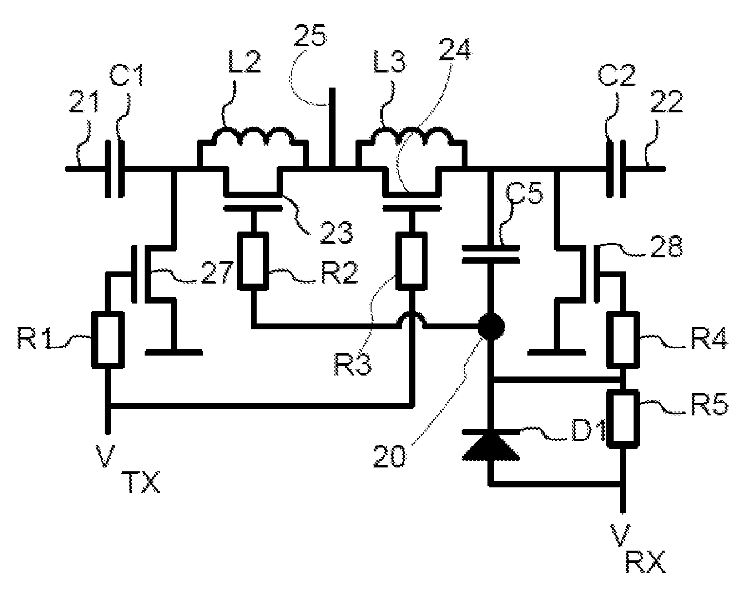
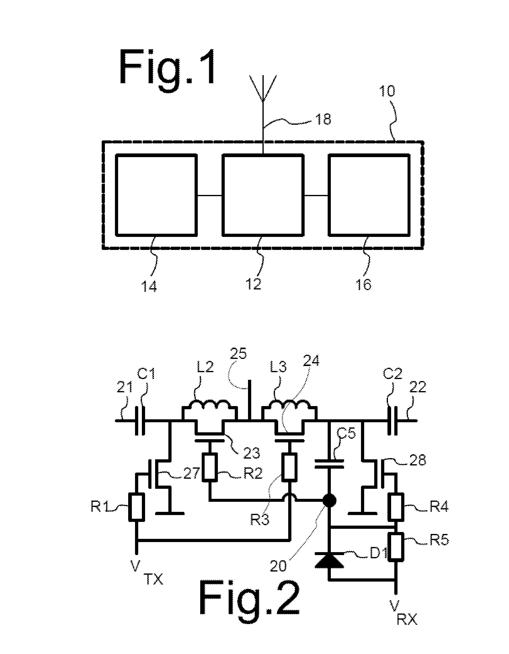
[0027]FIG. 1 shows an RF device 10 comprising a transmit / receive switch circuit 12, coupled to a transmitter 14, a receiver 16 and an antenna 18. FIG. 2 shows a schematic of a transmit / receive switch circuit. The transmit / receive switch circuit has a transmit input 21, a receive output 22, an antenna input / output 25 and a transmit control input VTX and a receive control input VRX. Although a circuit with an antenna is shown by way of example, it should be appreciated that a different signal source and sink may be coupled to input / output 25.

[0028]Transmit input 21 is coupled to antenna input / output 25 via a transmitter side circuit that comprises an input capacitor C1, an inductance L2 and a first and second transmitter side transistor 23, 27. Transmit input 21 is coupled to antenna input / output 25 via a series arrangement of input capacitor C1 and a main current channel of first transmitter side transistor 23. Inductance L2 is coupled in parallel to the main current channel of first...


PUM


Abstract

A transmit/receive switch circuit has a comprises a controllable transmit section and a controllable receive section, having an output and an input coupled to an RF transmit/receive terminal respectively. The transmit section comprises a first transistor having a main current channel coupled between an RF transmit signal input and the RF transmit/receive terminal. The receive section comprises a first transistor having a main current channel coupled between the RF transmit/receive terminal and a RF receive signal output and a second transistor having a main current channel coupled between the RF receive signal output and ground. A signal that is derived from an RF input signal at the RF transmit/receive terminal is rectified. The rectified signal is used to control a control electrode of the second transistor of the receive section to make this transistor increasingly conductive with increasing RF signal amplitude. The rectified signal may also be used to control a control electrode of the first transistor of the transmit section in this way. Thus, the transmit/receive switch circuit is made to perform a limiting function.

Description

[0001]This application is the U.S. National Phase of, and Applicants claim priority from, International Patent Application Number PCT / NL2012 / 050525 filed 20 Jul. 2012, which claims priority from EP 11174911.5 filed 21 Jul. 2011, each of which is incorporated herein by reference.BACKGROUND[0002]1. Field[0003]The invention relates to an RF device with a transmit / receive switch circuit.[0004]2. Description of the Related Art[0005]U.S. Pat. No. 5,689,818 discloses a transmit / receive switch circuit, i.e. a circuit that is able both to transmit signals to a terminal and receive signals from that terminal called a transmit / receive terminal. This circuit contains an RF transmit signal input; an RF receive signal output and the RF transmit / receive terminal. A transmit section has a first switching transistor between the RF transmit signal input and ground and a first pass switch coupled between the RF transmit signal input and the RF transmit / receive terminal. A receive section has a second ...

Claims


Application Information

Patent Timeline
IPC IPC(8): H04B1/44H04B1/48H04B1/10H03K17/693H03K17/0814H03K17/00
CPCH03K17/002H03K17/08142H03K17/693H04B1/109H04B1/48
Inventor VAN WANUM, MAURICE
Owner NEDERLANDSE ORG VOOR TOEGEPAST-NATUURWETENSCHAPPELIJK ONDERZOEK (TNO)
Why Eureka
Try Eureka