Touch device and manufacturing method thereof

a technology of a manufacturing method and a touch device, which is applied in the field of touch technology, can solve the problems of electrode cracking or delamination from the substrate, and may affect the production efficiency so as to reduce or eliminate the damage to the previously formed layer structure during the formation of the next layer thereon, and simplify the manufacturing process.

Active Publication Date: 2015-09-29
TPK TOUCH SYST XIAMEN
View PDF5 Cites 0 Cited by
  • Summary
  • Abstract
  • Description
  • Claims
  • Application Information

AI Technical Summary

Benefits of technology

[0007]The present disclosure provides a touch device and manufacturing method thereof wherein at least jumpers are formed by a transfer-printing process so as to reduce or eliminate damage to the previously formed layer structure during the formation of the next layer thereon, and therefore improving the yield.
[0010]According to the embodiments, at least the jumpers of the touch device are formed by the transfer-printing process, such that damage to the previously formed layer structure during the formation of the next layer thereon is reduced or eliminated and the yield is improved. In addition, using transfer-printing process instead of the sputtering, exposure and developing processes simplifies the manufacturing process and improve production efficiency. Moreover, the use of expensive equipment (such as the equipment for the sputtering, exposure and developing processes) is not required. As a result, price competitiveness is improved and the pollution caused by chemical solutions is, also reduced.

Problems solved by technology

However, in the above-mentioned method for manufacturing the touch device, the previously formed layer structure may be damaged during the formation of the next layer structure thereon.
For example, the electrodes may be cracked or delaminated from the substrate after undergoing several rounds of vacuum sputtering, exposure and developing processes.

Method used


Image

  • Touch device and manufacturing method thereof
  • Touch device and manufacturing method thereof
  • Touch device and manufacturing method thereof

Examples


Embodiment Construction

[0015]The following description is of the best-contemplated mode of carrying out the invention. This description is provided for the purpose of illustrating the general principles of the invention and should not be taken in a limiting sense. The scope of the invention is best determined by reference to the appended claims. Moreover, the same or similar elements in the drawings and the description are labeled with the same reference numbers.

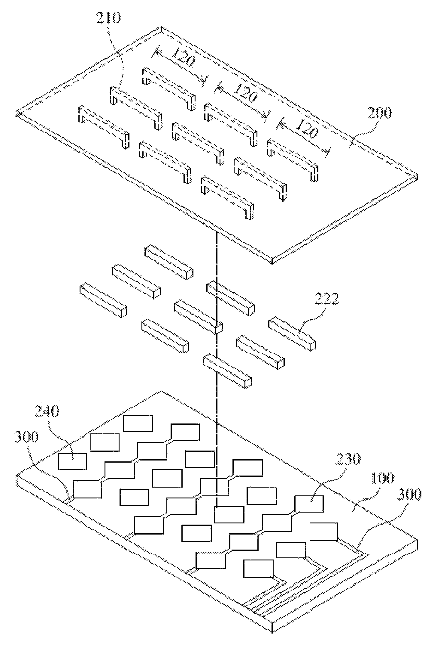
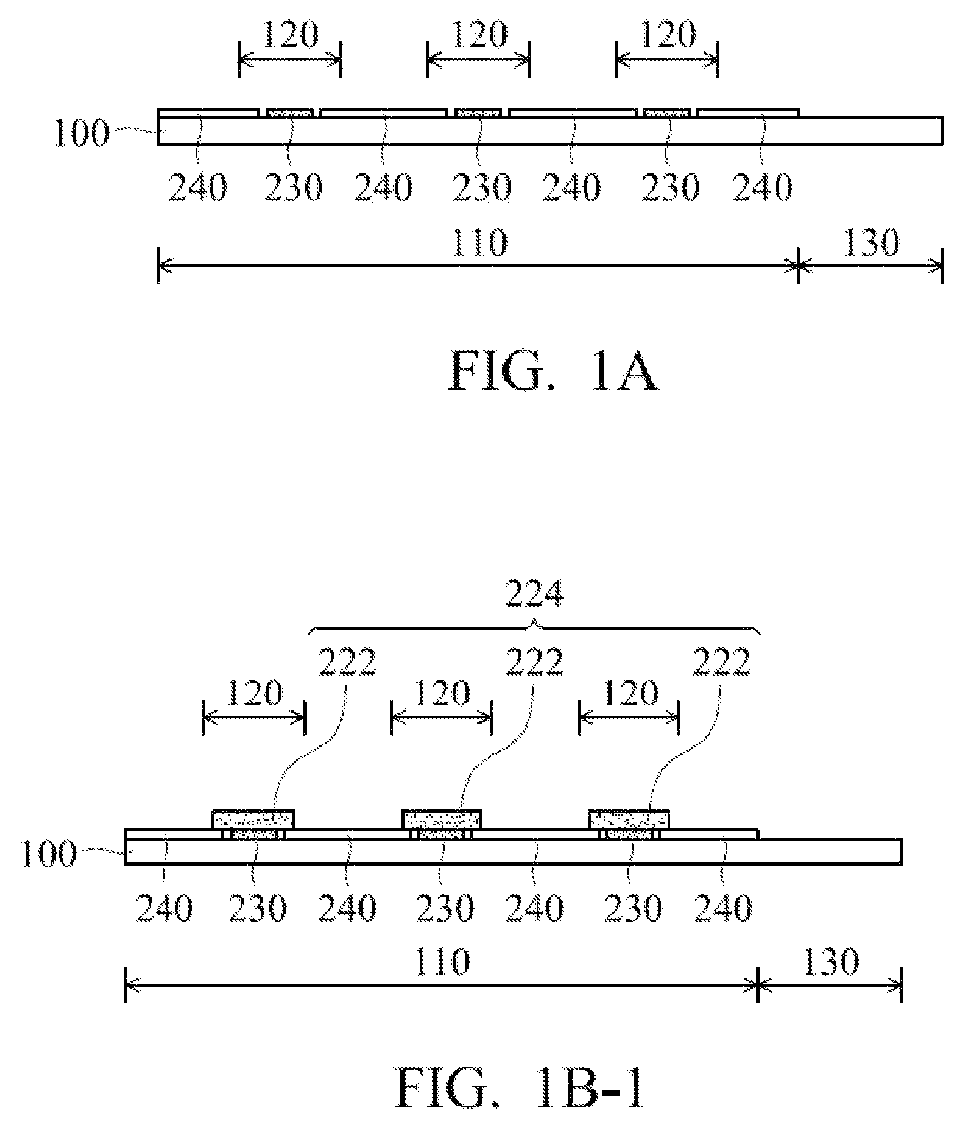
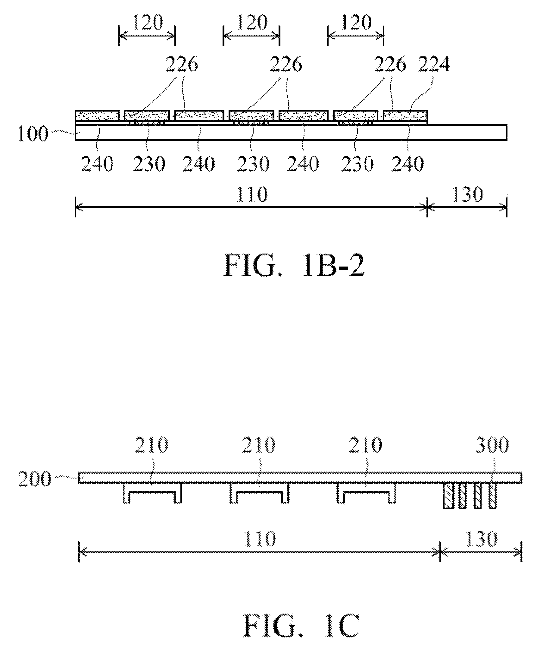
[0016]Referring to FIG. 1D-1 and FIG. 4, a cross-sectional view and an exploded view of an exemplary embodiment of a touch device according to the present disclosure are illustrated. In the present embodiment, the touch device comprises a substrate 100, a plurality of jumpers 210, an insulating layer 224, a plurality of first sensing electrodes 230, a plurality of second sensing electrodes 240 and a transfer-printing film 200. The substrate 100 has a viewing region 110. The first sensing electrodes 230 and the second sensing electrodes 240 are ins...


PUM

PropertyMeasurementUnit
thicknessaaaaaaaaaa
thicknessaaaaaaaaaa
conductivityaaaaaaaaaa

Abstract

A manufacturing method of a touch device is disclosed. A substrate having a viewing region is provided. A plurality of first sensing electrodes and a plurality of second sensing electrodes insulated from and in a staggered arrangement with the plurality of first sensing electrodes are formed on the substrate corresponding to the viewing region, wherein a plurality of jumper regions are defined between the adjacent second sensing electrodes. An insulating layer is formed on the plurality of first sensing electrodes and the plurality of second sensing electrodes. A plurality of jumpers is transfer-printed onto the insulating layer, wherein the plurality of jumpers is electrically connected to the adjacent second sensing electrodes and insulated from the first sensing electrodes by the insulating layer. A touch device is also disclosed.

Description

BACKGROUND OF THE DISCLOSURE[0001]All related applications are incorporated by reference. The present application is based on, and claims priority from, China Application Serial Number No. 201210388195.2, filed on Sep. 27, 2012, the disclosure of which is hereby incorporated by reference herein in its entirety.FIELD OF THE DISCLOSURE[0002]The present disclosure relates to touch technology, and in particular to a touch device and manufacturing method thereof.DESCRIPTION OF THE RELATED ART[0003]With the developments in the field of information technology, touch devices increasingly used to provide a convenient way to deliver information between humans and machines. A typical touch device is formed by a plurality of electrodes in the x-direction and a plurality of electrodes in the y-direction in a staggered arrangement. For example, the electrodes in the x-direction and the electrodes in the y-direction are disposed on the same side of a transparent substrate. Jumpers are connected to...

Claims


Application Information

Patent Timeline
Patent Type & Authority Patents(United States)
IPC IPC(8): H03K17/975H03K17/96G06F3/044H01H11/00
CPCH03K17/9622G06F3/044H01H11/00G06F2203/04103G06F2203/04111Y10T29/49105G06F3/0443G06F3/0446
Inventor CHANG, HENG-YAOCHANG, CHEN-HSINWU, MENGH-SUEHWU, CHE-LCHEN, LIXIAN
Owner TPK TOUCH SYST XIAMEN
Why Eureka
Try Eureka